3 a/d data register (adcr0/adcr1), A/d data register (adcr0/adcr1), 0/adcr1 – FUJITSU F2MCTM-16LX User Manual
Page 367
351
CHAPTER 18 8-/10-BIT A/D CONVERTER
18.3.3
A/D Data Register (ADCR0/ADCR1)
The A/D data register (ADCR0/ADCR1) stores the digital value generated as the
conversion result. The ADCR0 stores the lower 8-bit, and ADCR1 stores the most
significant 2-bit of the conversion result. This register is rewritten each time the
conversion complete and stores last conversion value normally.
■
A/D Data Register (ADCR0/ADCR1)
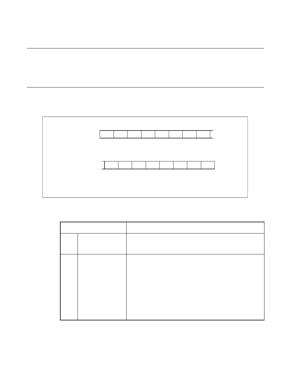
Figure 18.3-4 A/D Data Register (ADCR
0/ADCR1
)
R
R
R
R
R
R
R
R
R
R
XXXXXX00
B
0 0 0 0 0 0 0 0
B
R
X
-
15
14
13
12
11
10
9
8
00006B
H
-
-
-
-
-
ADCR1
00006A
H
ADCR0
7
6
5
4
3
2
1
0
D7
D6
D5
D4
D3
D2
D1
D0
-
-
-
-
-
-
-
D9
D8
Reset value
Reset value
Data register (High)
Address
Data register (Low)
Address
: Read only
: Undefined bit
: Indeterminate
Table 18.3-4 Functions of A/D Data Register (ADCR0/ADCR1)
Bit Name
Function
bit15
to
bit10
Undefined bits
1 is always read at reading.
bit9
to
bit0
D9 to D0:
A/D conversion data
bits
These bits store the A/D conversion results.
When resolution set in 10 bits (S10=0):
Conversion data is stored in the 10 bits from D9 to D0.
When resolution set in 8 bits (S10=1):
Conversion data is stored in the 8 bits from D7 to D0. In this
case, the read values of D9 and D8 are 1.
Note:
•
Writing to this register is disabled.
•
Use a word instruction (MOVW) to read the A/D conversion
results stored in the A/D conversion data bits (D9 to D0).