Block diagram of flash/mask rom version – FUJITSU F2MCTM-16LX User Manual
Page 27
11
CHAPTER 1 OVERVIEW
■
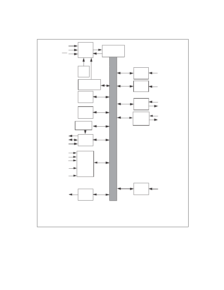
Block Diagram of Flash/Mask ROM Version
Figure 1.2-3 Block Diagram of Flash/Mask ROM Version
AN15 to AN0
Clock
control/
monitor
*
3
RAM
3KB
ROM
64KB
UART
2 channels
8/16bit
PPG
2 channels
F2MC-16LX core
Input
capture
4 channels
16-bit
I/O
timer 0
CAN
controller
1 chnnal
16-bit
reload
timer
2
channels
DTP/
external
interrupt
SOT0,SOT1
SCK0,SCK1
SIN0,SIN1
PPGF(E),PPGD(C),
PPGC(D),PPGE(F)
IN0 to IN3
FRCK0
RX1
TX1
TIN2,TIN3
TOT2,TOT3
INT8,INT9R
INT10,INT11
INT12R,INT13
INT14R,INT15R
CPU operation
detection*
2
Low voltage
detection*
2
CR
oscillation
circuit
Internal data bus
AV
SS
AV
CC
Prescaler
(2 channels)
8/10-bit
A/D
converter
16 channels
X0,X1
X0A,X1A *
1
RST
AVR
ADTG
*1: Product without S-suffix
*2: Product with T-suffix
*3: CR oscillation circuit/clock supervisor supports MB90367/T(S), MB90F367/T(S) only
- XG Series P3NK-4452-01ENZD (614 pages)
- FPCAC14C (1 page)
- MCJ3230SS (161 pages)
- MBA3073NC (138 pages)
- T5140 (102 pages)
- T5140 (76 pages)
- MAM3367MC/MP (152 pages)
- MPC3045AH (185 pages)
- MB2142-02 (23 pages)
- MB15F86UL (6 pages)
- MHS2030AT (40 pages)
- MHW2100BS (296 pages)
- MHK2060AT (227 pages)
- Disk Drives MHK2060AT (227 pages)
- MCM3064SS (170 pages)
- Mainboard D1561 (45 pages)
- MHC2040AT (219 pages)
- D1961 (45 pages)
- DISK DRIVES MHM2100AT (231 pages)
- MHR2010AT (250 pages)
- MHZ2120BJ (320 pages)
- MCE3064AP (175 pages)
- LQFP-64P (16 pages)
- Solaris PCI GigabitEthernet 3.0 (115 pages)
- MAY2036RC (94 pages)
- MAB3091 (142 pages)
- MPE3XXXAT (191 pages)
- MHV2040AH (40 pages)
- MHW2040AC (278 pages)
- ETERNUSmgr P2X0-0202-01EN (64 pages)
- VSS Hardware Provider 2.1 (134 pages)
- MAG3182FC (61 pages)
- MAU3147NC/NP (130 pages)
- MAX3147RC (94 pages)
- MHV2160BT (296 pages)
- MHV2040AT (280 pages)
- MAW3300NC/NP (130 pages)
- DeskPower E623 (50 pages)
- MAG3182LC (133 pages)
- OPTICAL DISK DRIVES MDG3064UB (42 pages)
- MHF2021AT (225 pages)
- MHR2040AT (40 pages)
- Single Drive FTM7926FB (1 page)
- PG-FCS103 (98 pages)
- MAS3735FC (114 pages)