Block diagram of address match detection function – FUJITSU F2MCTM-16LX User Manual
Page 523
507
CHAPTER 22 ADDRESS MATCH DETECTION FUNCTION
22.2
Block Diagram of Address Match Detection Function
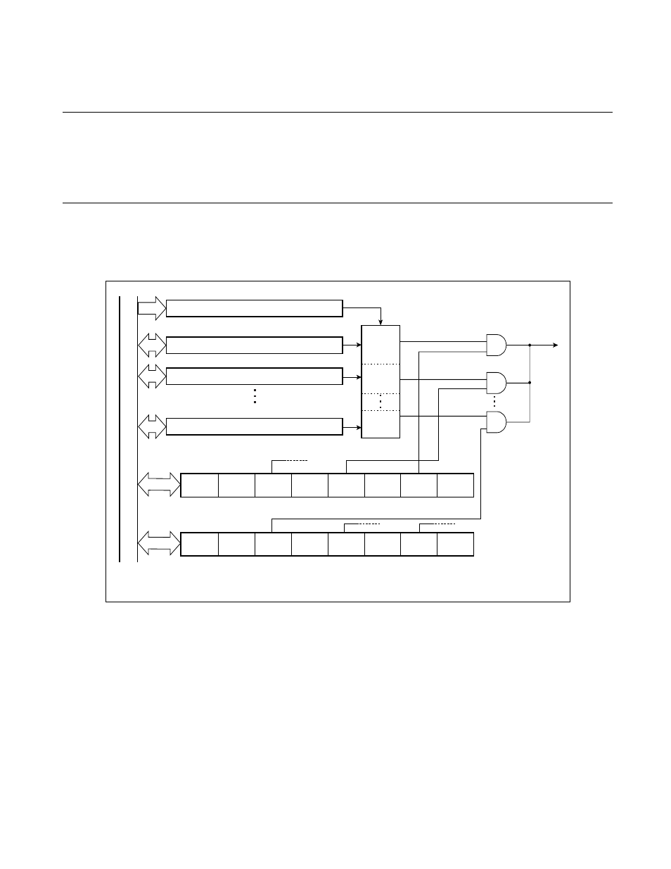
The address match detection module consists of the following blocks:
• Address latch
• Address detection control register (PACSR0/PACSR1)
• Detect address setting registers (PADR0 to PADR5)
■
Block Diagram of Address Match Detection Function
Figure 22.2-1 shows the block diagram of the address match detection function.
Figure 22.2-1 Block Diagram of the Address Match Detection Function
●
Address latch
The address latch stores the value of the address output to the internal data bus.
●
Address detection control register (PACSR0/PACSR1)
The address detection control register enables or disables output of an interrupt at an address match.
●
Detect address setting registers (PADR0 to PADR5)
The detect address setting registers set the address that is compared with the value of the address latch.
AD1E
AD2E
AD0E
PACSR0
AD4E
AD5E
AD3E
PACSR1
Address latch
Detection address setting register 0
PADR0 (24 bits)
PADR1 (24 bits)
PADR5 (24 bits)
Detection address setting register 1
Detection address setting register 5
Comparator
INT9 instruction
(INT9 instruction
generation)
Reserved
Inte
rn
al
dat
a b
u
s
Address detection control register 0 (PACSR0)
Address detection control register 1 (PACSR1)
Reserved: Always setting to 0.
Reserved
Reserved
Reserved
Reserved
Reserved Reserved
Reserved
Reserved
Reserved