2 clock selection, Figure 4-11, Functional description – Artesyn ARTM-831X Installation and Use (June 2014) User Manual
Page 83
Functional Description
ARTM-831X Installation and Use (6806800M76E)
83
The first one is routed via the upper mezzanine connector to the ARTM-831X_base unit and
connected to the FPGA_base device. It allows access to the mezzanine expansion section of
this FPGA_base device.
The second one is routed to its companion, the TSI- extender FPGA. It allows transparent access
to the registers in this device and thus the connected signals. The clock of this I/F is used as
master clock for the companion.
The third SPI is used for configuration and connects to a SPI Flash device.
For details, see
Figure "ARTM-831X SPI Bus & RESET Structure" on page 65
4.4.1.2
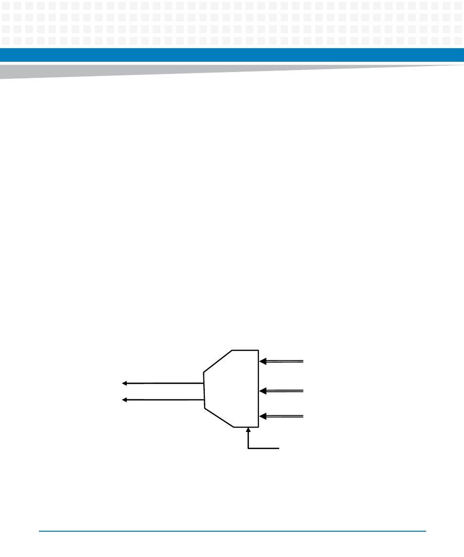
Clock selection
The DS3/OC3 mezzanine expansion unit provides a programmable reference clock selector
unit. The TSI-FPGA device provides clock selection for the SONET/SDH/DS3 framer 0/1 and the
E1/T1 framer devices 0/1. Two reference clocks out of various recovered receive clocks are pre-
selected and routed to the ARTM-831X base unit via the upper mezzanine connector. At the
ARTM-831X base unit they are connected to the clock selection unit in the FPGA-base device
and depending on its configuration forwarded to the system synchronizer located at the front
board. Each of the inputs is masked on respective LOS alarm.
Figure 4-11 DS3/OC3 mezzanine TSI-FPGA recovered receive clock selector unit
TDM RefCLK 0
TDM_RefCLK_1
To
ba
se bo
ard
vi
a
upp
er me
zza
ni
ne
conn
ect
o
r
16x recovered receive CLK
from E1/T1 Framer
8x SONET/SDH recovered
clock (working)
8x recovered T1/E1 payload clocks
from SONET/SDH Framers
Mask input on respective LOS Alarm