Table 9-21, Tsi channel mapping, Tsi fpga – Artesyn ARTM-831X Installation and Use (June 2014) User Manual
Page 290
TSI FPGA
ARTM-831X Installation and Use (6806800M76E)
290
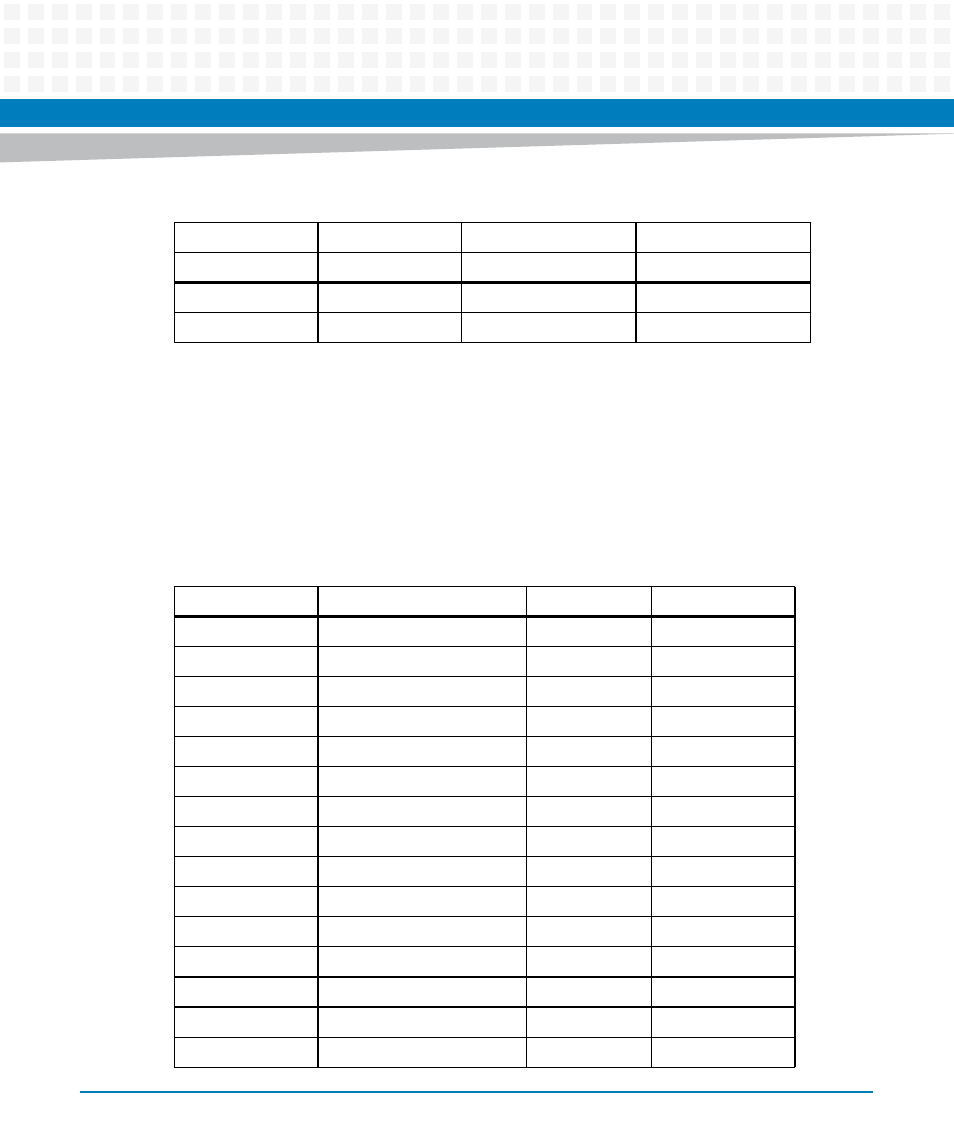
Each of the 16 bit address of the TSI connection memory (CM) represents one of the incoming
data channel. To connect one channel to the other the connection memory has to be written
with the 16 bit address of the outgoing channel, e.g. if the incoming data of channel 0x1234
have to be forwarded to channel 0x5678 the CM at address 0x5678 has to be set to the value
0x1234.
0x27FE
0xFFF1
+8
-
0x27FF
0xFFF9
+8
-
Table 9-21 TSI Channel Mapping
Mask (16 bit)
First channel
Cycle
Channel 0
xxxx xx00 0000 0000
0x0000
1024
DSP 0 (SerDes)
xxxx xxxx xxxx x001
0x0001
1024/128 = 8
xxxx xxxx xxx0 0100
0x0004
1024/32 = 32
DSP 1 (SerDes)
xxxx xxxx xxxx x010
0x0002
1024/128 = 8
xxxx xxxx xxx0 1100
0x000C
1024/32 = 32
DSP 2 (SerDes)
xxxx xxxx xxxx x101
0x0005
1024/128 = 8
xxxx xxxx xxx0 1000
0x0008
1024/32 = 32
SBI 0
xxxx xxxx xxxx x011
0x0003
1024/128 = 8
xxxx xxxx xx11 1100
0x003c
1024/16 = 64
xxxx xxxx x001 1100
0x001c
1024/8= 128
SBI 1
xxxx xxxx xxxx x111
0x0007
1024/128 = 8
xxxx xxxx xx10 0000
0x0020
1024/16 = 64
xxxx xxxx x011 1000
0x0038
1024/8= 128
GR8
xxxx xxxx xx11 0100
0x0034
1024/16 = 64
HMVIP 0
xxxx xxxx 0001 0000
0x0010
1024/4 = 256
Table 9-20 TSI channel map for DSP 0 (SerDes) block (continued)
DSP 0
TSI
cycle
cycle
channel sequence
channel sequence
slice of 128x64 channel slice of 32x64 channel