5 rtm fpga hw/sw interfaces, 1 rtm fpga address map overview, Table 9-5 – Artesyn ARTM-831X Installation and Use (June 2014) User Manual
Page 171: Rtm fpga address map overview
TSI FPGA
ARTM-831X Installation and Use (6806800M76E)
171
9.5
RTM FPGA HW/SW Interfaces
9.5.1
RTM FPGA Address map Overview
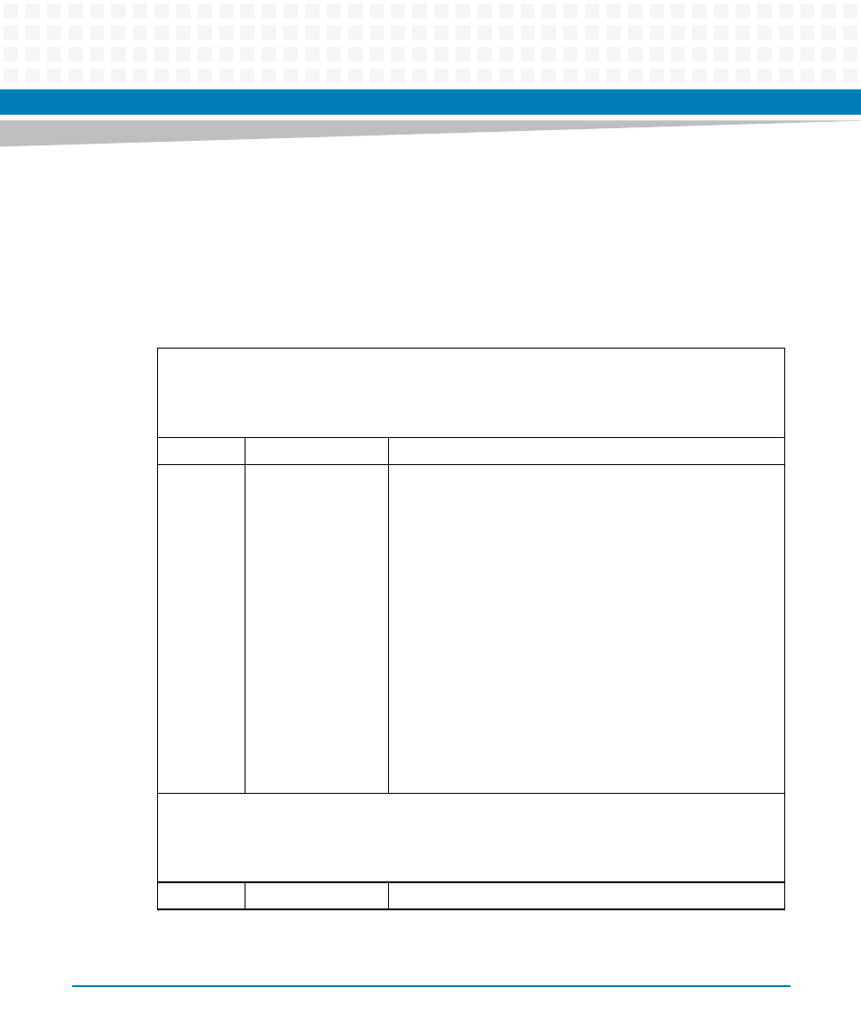
Table 9-5 RTM FPGA Address map Overview
TSI Memory (TsiMem) [Hw: Cy0, InR, OutR]
The connection memory of the TSI is accessible to switch connections.
Access via PCI-bus 512kByte prefetchable memory area of 64bit-bar[1,0], hereof assigned to this
block: 0...3FFFF
Address
Acronym
Description
0x0
...
0x3FFFC
TsiCnctMem0
...
TsiCnctMem65535
Tsi Connection Memory (32bit)
The lower 16bit value of TsiCnctMem cell 0 determines the
input channel to which output channel 0 is connected,
the lower 16bit value of TsiCnctMem cell 1 determines the
input channel to which output channel 1 is connected, etc.
Setting Bit 16 results in discarding the output data of the TSI
interchange data memory and substituting it with the data
in the lower 8 bit of this connection memory entry, e.g:
Value 0x00001 at address 0x00005 connects TSI input channel
1 to output channel 5,
value 0x10001 at address 0x00005 causes static idle pattern
0x01 to be output at channel 5.
Bit 17 of the Memory cells is read as written and has no
influence on HW.
It can be used by SW to store other channel associated
information.
GR8 Memory (Gr8Mem) [Hw: Cy0, InR, OutR]
The connection memory of the TSI is accessible to switch connections.
Access via PCI-bus 512kByte prefetchable memory area of 64bit-bar[1,0], hereof assigned to this
block: 40000...7FFFF
Address
Acronym
Description