2 clock selection, 3 local bus, 4 tsip2serdes interface – Artesyn ARTM-831X Installation and Use (June 2014) User Manual
Page 76: Figure 4-8, Functional description
Functional Description
ARTM-831X Installation and Use (6806800M76E)
76
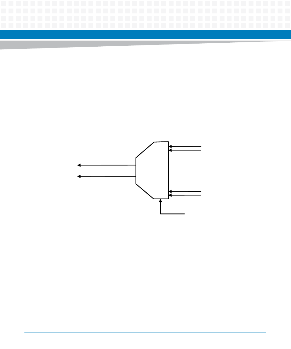
4.3.1.2
Clock Selection
The E1/T1 mezzanine expansion unit provides a programmable reference clock selector unit.
The TSI-FPGA device provides clock selection for the Framer 0 and 1. Two reference clocks out
of 16 recovered receive clocks are pre-selected and routed to the ARTM-831X base unit via the
upper mezzanine connector. At the ARTM-831X base unit they are connected to the clock
selection unit in the FPGA-base device and depending on its configuration forwarded to the
system synchronizer located at the front board. Each of the inputs is masked on respective LOS
alarm.
4.3.1.3
Local Bus
To provide host access to the Framer and LIU devices, the TSI-FPGA implements a PCIexpress
to Local Bus Bridge. The Local Bus Interface is an asynchronous, parallel, non-multiplexed,
memory mapped interface for I/O read and write operations according to Intel bus mode. A
data bus width of 8Bit is used on the E1/T1 mezzanine.
4.3.1.4
TSIP2SERDES Interface
The data transport for the TDM channels happens via the proprietary TSIP interface. To reduce
pin count, the TSI-FPGA employs a hi-speed serialized interface (TSIP-to-SerDes) unit. Three
separate SerDes lanes are available to support the front board DSP module slots (onboard and
2 expansion slots).
Figure 4-8
E1/T1 mezzanine TSI-FPGA recovered receive clock selector unit
TDM RefClk 0
TDM_RefClk_1
To
ba
se bo
ard
vi
a
upp
er me
zza
ni
ne
conn
ect
o
r
16x recovered receive CLK
from E1/T1 Framer
Mask input on respective LOS Alarm
. . . . . . . .