Tsi fpga – Artesyn ARTM-831X Installation and Use (June 2014) User Manual
Page 280
TSI FPGA
ARTM-831X Installation and Use (6806800M76E)
280
9.5.2.14.2 Configuration Prom Update Data Register
Address:
0x2001, CfgPrmUpdDatReg
Width: 8 bit
Holds the write data to sent to the FPGA serial configuration prom when written and the read
data received from the FPGA serial configuration prom when read.
9.5.2.15 External components accessed through RTM FPGA as bridge to SPI bus 1
(ExtBridgedCompSpi1)
The RTM Fpga bridges the PCI Bus to SPI Bus 1. The SPI interface of the ExtFpga on the RTM-
Module components is connected to this bus. The bus width is adapted automatically to the
needs of the accessed component.
9.5.2.16 External components accessed through RTM FPGA as bridge to SPI bus 2
(ExtBridgedCompSpi2)
The RTM Fpga bridges the PCI Bus to SPI Bus 2, HW signals are used commonly with SPI Bus
3(multiplexed). The SPI interfaces to a BaseExtFpga components which us connected to this
bus. The bus width is adapted automatically to the needs of the accessed component.
9.5.2.17 External components accessed through RTM FPGA as bridge to SPI bus 3
(ExtBridgedCompSpi3)
The RTM Fpga bridges the PCI Bus to SPI Bus 3, HW signals are used commonly with SPI Bus 2
(multiplexed). The SPI interfaces to 2x DS26503 components which are connected to this bus.
The BaseExtFpga routes the Spi-Bus directly to the Ds26503 components and bypasses its
internal bus. The bus width is adapted automatically to the needs of the accessed component.
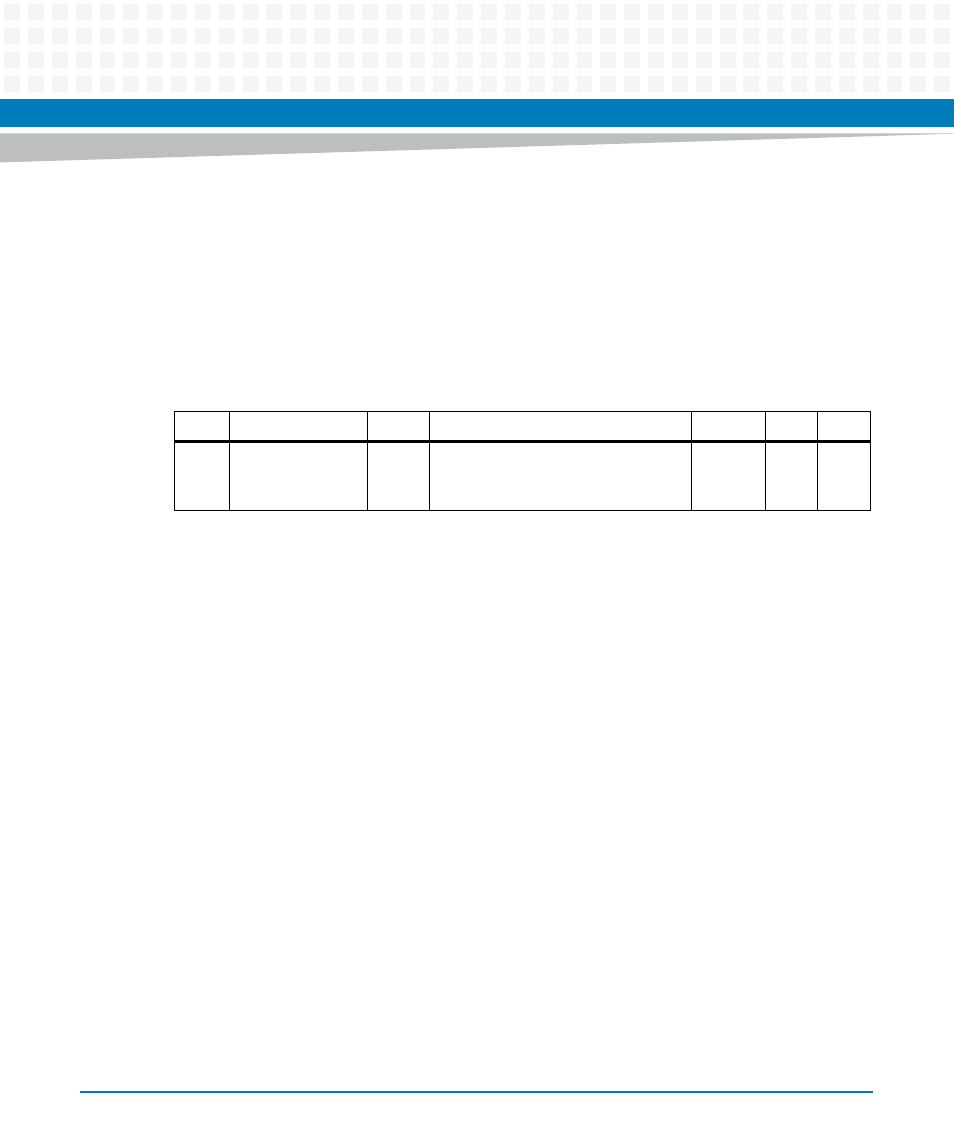
Bit
Acronym
Type
Description
Default
Pwr
Soft
7...0
CfgSerialPrmDat
RorW
A write triggers 8 SPI clocks and
shifts the data out to MOSI. The Data
on MISO is shifted in.
0x0
X
-