2 ref clock selection, 3 register description, 2 ref clock selection 4.2.1.3 register description – Artesyn ARTM-831X Installation and Use (June 2014) User Manual
Page 68: Figure 4-6, Fpga_base recovered receive clock selector unit, Functional description
Functional Description
ARTM-831X Installation and Use (6806800M76E)
68
The IP overhead signals are routed to the FPGA_base device:
SFP+ I2C control (FPGA I/O)
I2C slave for IPMC access (FPGA(I/O)
Loss of signal; Loss of lock (FPGA input)
Transmitter disable (FPGA I/O)
SFP present (FPGA input)
Copper Reference Clock Lock (FPGA input)
BITS Loss of frame, Loss of Signal, RAIS (FPGA input)
4.2.1.2
Ref Clock Selection
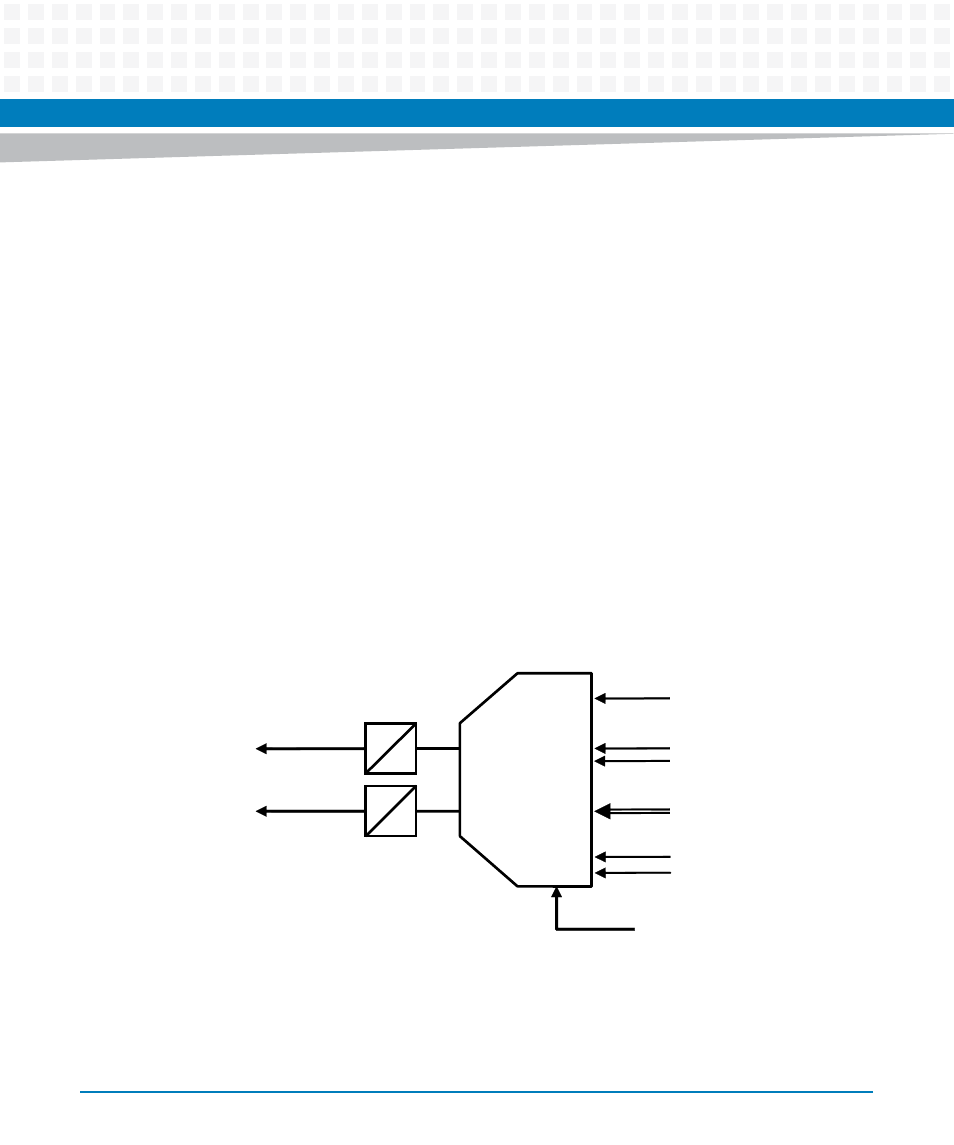
The FPGA_base provides a programmable reference clock selector unit that allows to select
between various recovered receive clocks. Two of these are routed as reference clocks to the
system synchronizer located at the front board. Each of the inputs can be masked by a
corresponding alarm.
4.2.1.3
Register Description
For register Description, see
Chapter 8, Registers, on page 128
Figure 4-6
FPGA_base recovered receive clock selector unit
RefCLK 1
RefCLK_2
To fro
n
t bo
ard
vi
a
zone
3
con
nec
tor
125MHz recovered receive
CLK from 10GbE I/F
2x 25MHz recovered receive
CLK from 1GbE I/F
Configurable
dividers
4x recovered receive CLK
from TDM mezzanine
2x T1/E1 recovered receive
CLK from BITS I/F (T3 CLK)
Mask input on respecitve LOS Alarm
Clock
Selector