1 artm base fpga register overview, Table 8-23, Register access type – Artesyn ARTM-831X Installation and Use (June 2014) User Manual
Page 129: Table 8-24, Artm base fpga register overview, Base artm fpga
Base ARTM FPGA
ARTM-831X Installation and Use (6806800M76E)
129
8.3.1
ARTM Base FPGA Register Overview
All addresses not listed in the
Table "ARTM Base FPGA Register Overview" on page 129
are
reserved. A write to one of these addresses is ignored.
The Address Map for all other Registers (TDM Registers) accessed by Mezzanine SPI Interface.
This Address Map has Sub-Version Register which is incremented with the ARTM Base FPGA
Code Main-Version (
) in the case the corresponding code has changed.
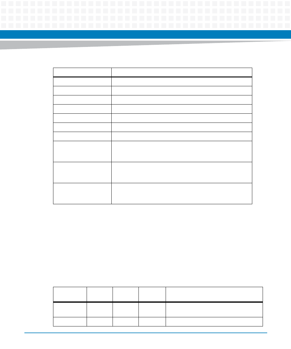
Table 8-23 Register Access Type
Access
Description
r
Read only
w
Write only
r/w
Read and write
w1c
Write-1-to-clear, ignore bit while reading
r/w1c
Read and write-1-to-clear, write 0 has no effect
r/w1s
Read and write-1-to-set, write 0 has no effect
r/w1t
Read and write-1-to-toggle, write 0 has no effect
RTM:
The prefix "RTM:" signals that the access is restricted to the RTM SPI
interface. For example, RTM: r/w means that the register bit is
read/writable from the ATCA board via RTM SPI interface
SPI:
The prefix "SPI:" signals that the access is restricted to the
Mezzanine SPI Interface.For example, SPI: r/w means that the
register bit is read/writable from the Mezzanine SPI Interface.
MMC:
The prefix "MMC:" signals that the access is restricted to the MMC
I2C interface. For example, MMC: r/w means that the register bit is
read/writable from the MMC I2C interface.
Table 8-24 ARTM Base FPGA Register Overview
Address /
Range
RTM SPI
SPI Mezz
MMC I2C
Description
0x0
x
x
x
ARTM Base FPGA Code Main-Version (Table
261)
0x1
x
SFP I2C select Register