Figure 9-4, Cm (connection memory) data, Tsi fpga – Artesyn ARTM-831X Installation and Use (June 2014) User Manual
Page 164
TSI FPGA
ARTM-831X Installation and Use (6806800M76E)
164
The TSI Channel Supervisor addresses (derived from the TSI Slot Counter) the interface blocks
connected as peripherals of the TSI. Each of theses blocks (SBI 0..1, HMVIP 0..5 …) is connected
by a separate 8 bit TDM buss along with enable signal for output or input of data.
The TSI Channel Supervisor distributes the TSI-channels in a minimum granularity of 64
channels per time frame to the connected input/output blocks (refer to chapter 1.6 TSI channel
mapping). All interface blocks and components before or after this blocks are adjusted in terms
of delay in a way that their speech data arrives exactly in phase with frame start of the TSI Slot
Counter. In the other direction they are adjusted to accept data exactly in phase with frame
start of the TSI Slot Counter at the output TDM bus.
The TSI core consists out of a structure of dual ported memories. To obtain the necessary
output data rate of the TSI the dual ported speech memories are read out via both ports and
with four channels in parallel.
To guarantee that every switched channel output data of the TSI belongs to the same time
frame of the input data the SM (speech memory) is doubled. During a time frame of 125μs data
input is written to one part of the SM and output data are read out of the other part of the SM.
The memories change their role with each new time frame.
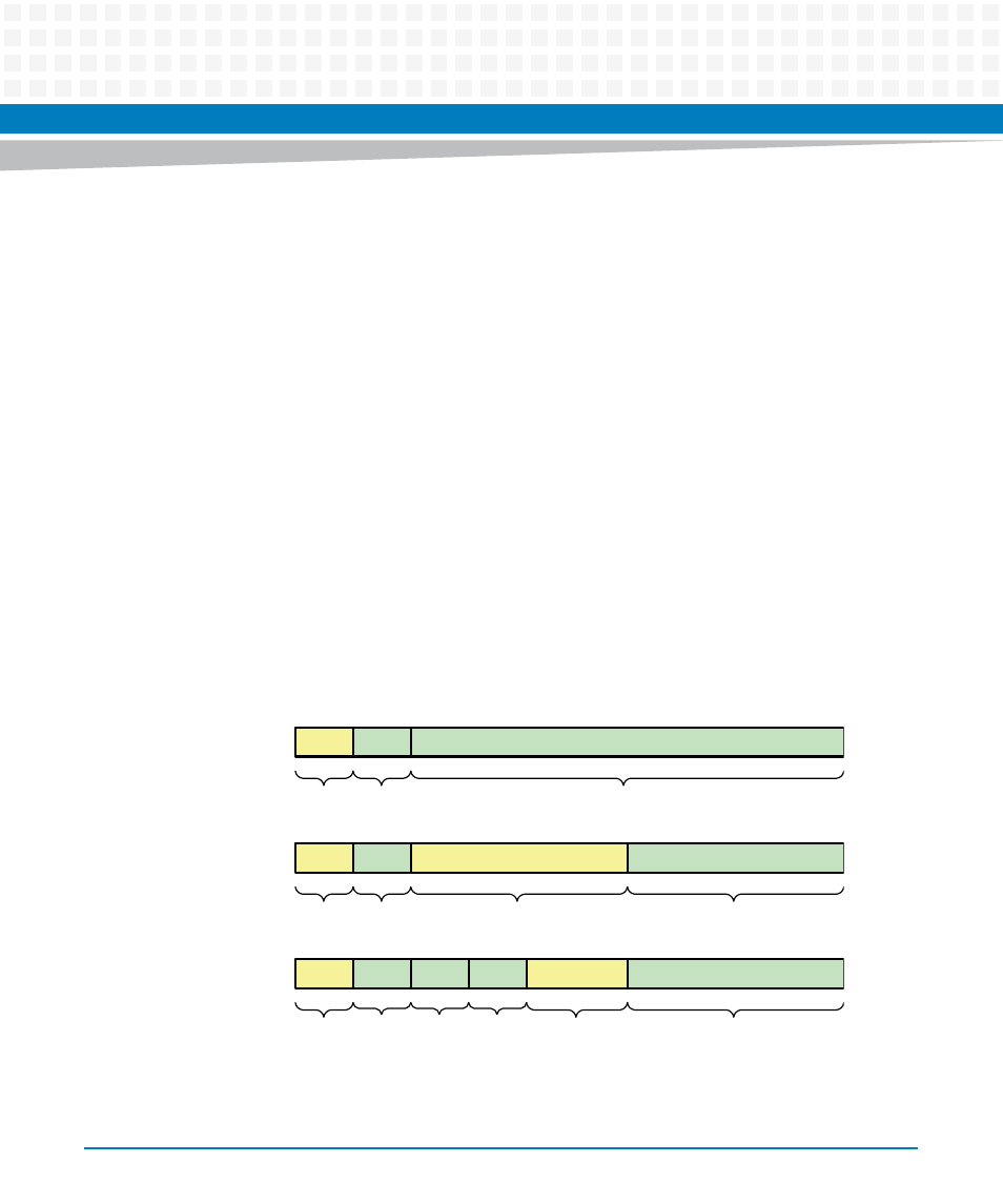
Figure 9-4
CM (connection memory) data
tbd
fixed pattern bits
16 bits
1 bit
1
1 bit
fixed
pattern
tbd
connected channel
0
15
0
16
17
switch
channel
0
15
16
17
1 bit
1 bit
don’t care
8 bits
8 bits
tbd
fixed pattern bits
1 bit
1
1 bit
fixed
pattern for SBI
interface
0
15
16
17
don’t care
6 bits
8 bits
SAPL
SAV5
14
1 bit
1 bit