Avago Technologies LSI53C1010R User Manual
Page 115
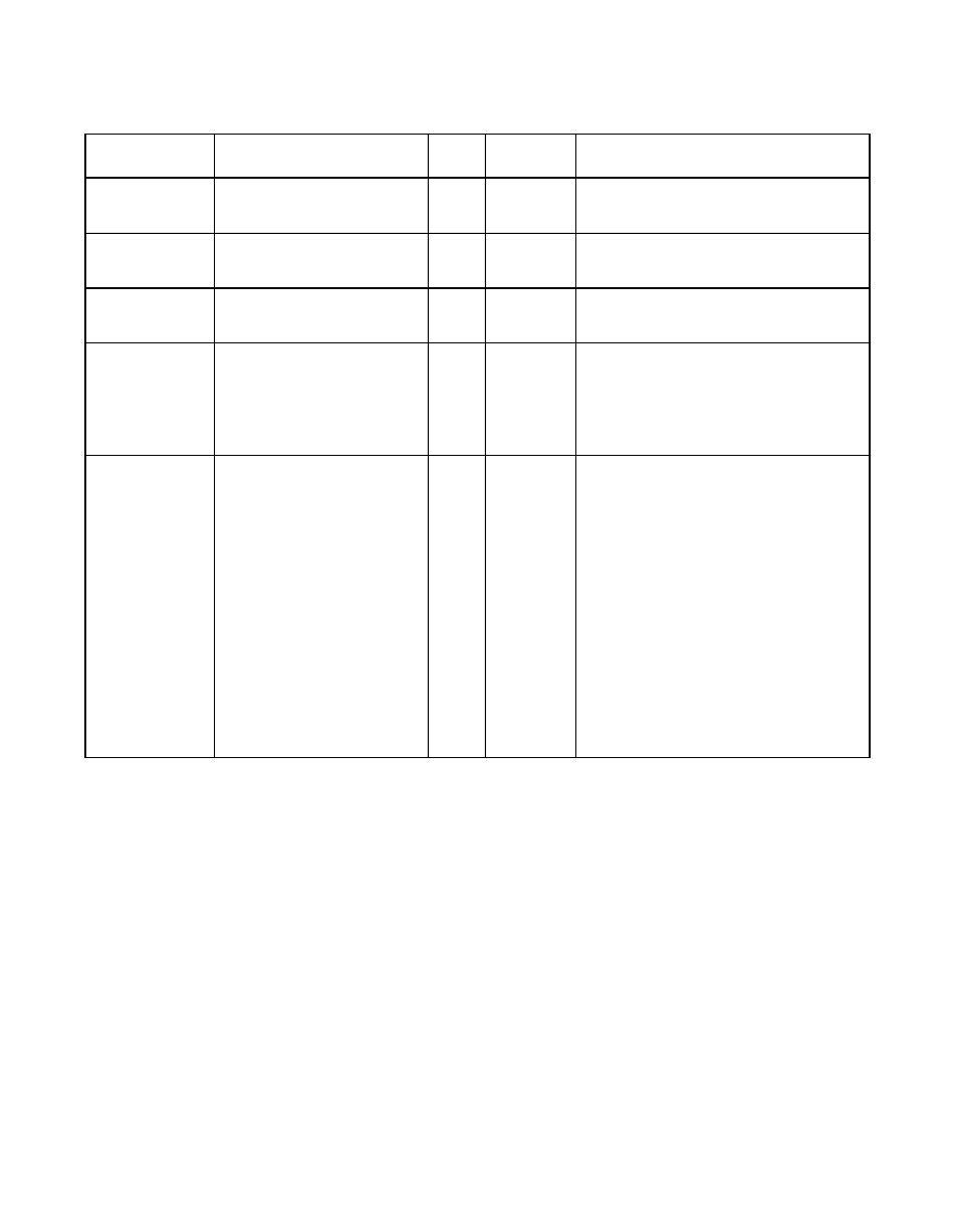
Power and Ground Signals
3-21
Version 2.2
Copyright © 2000–2003 by LSI Logic Corporation. All rights reserved.
VSSA
AB6, H5
G
N/A
Ground for analog cells (clock
quadrupler and DIFFSENS logic).
A_VDDBIAS
T1
P
N/A
Power for the SCSI Function A
RBIAS.
B_VDDBIAS
B13
P
N/A
Power for the SCSI Function B
RBIAS.
B_RBIAS
A11
I
N/A
Connects an external resistor to
generate the LVDlink pad bias
current. The resistor value should be
10 k
Ω
. Connect the other end of the
resistor to V
DD
.
NC
A24, B2, B3, B23, B24,
B25, C2, C3, C5, C14,
C22, C24, C25, D4, D5,
D15, D20, D21, D22,
D23, E3, E4, E5, E6, E20,
E21, E22, E23, E24, F4,
F5, F22, G5, M23, N2,
N23, P2, R1, W25, Y5,
Y22, AA4, AA5, AA22,
AB3, AB4, AB5, AB21,
AB22, AC4, AC10, AC22,
AC23, AD2, AD3, AD9,
AD14, AD18, AD24, AE5,
AE6, AE25, AF4, AF12,
AF15
N/A
N/A
These pins are reserved or have no
internal connection.
1. The I/O driver pad rows and digital core have isolated power supplies as indicated by the “I/O” and
“CORE” extensions on their respective V
SS
and V
DD
names. Connect the power and ground pins
directly to the primary power and ground planes of the circuit board. Apply bypass capacitors of
0.01
µ
F between adjacent V
SS
and V
DD
pairs wherever possible. Do not connect bypass capacitors
between V
SS
and V
DD
pairs that cross power and ground bus boundaries.
2. To reduce signal noise that can affect Frequency Synthesizer (FSN) functionality, place a ferrite
bead in series with the V
DDA
and V
SSA
pins. The recommended rating of the bead is 150
Ω
at
100 MHz.
Table 3.17
Power and Ground Signals (Cont.)
Name
1
Bump
Type
Strength
Description