8 power and ground signals, Table 3.17 power and ground signals, Power and ground signals – Avago Technologies LSI53C1010R User Manual
Page 114: Section 3.8, “power and ground signals
3-20
Signal Descriptions
Version 2.2
Copyright © 2000–2003 by LSI Logic Corporation. All rights reserved.
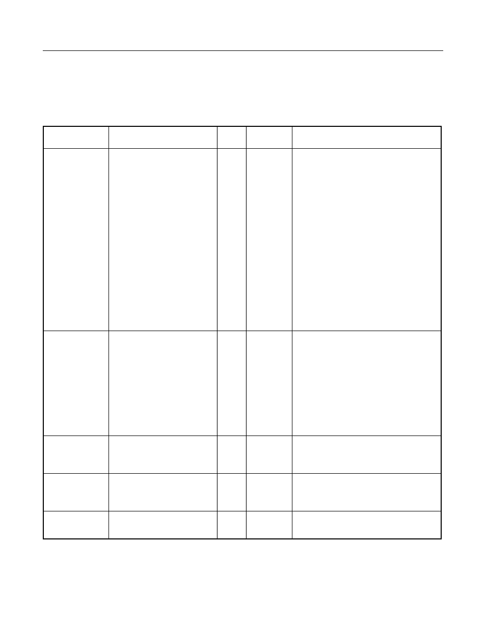
3.8 Power and Ground Signals
describes the Power and Ground Signals group.
Table 3.17
Power and Ground Signals
Name
1
Bump
Type
Strength
Description
VSS_IO
A5, A9, A13, A17, A21,
A25, B1, B26, C4, C8,
C12, C16, C20, D24, E1,
F26, G3, H24, J1, K26,
L3, L11, L12, L13, L14,
L15, L16, M11, M12,
M13, M14, M15, M16,
M24, N1, N11, N12, N13,
N14, N15, N16, P11, P12,
P13, P14, P15, P16, P26,
R3, R11, R12, R13, R14,
R15, R16, T11, T12, T13,
T14, T15, T16, T24, U1,
V26, W3, Y24, AA1,
AB26, AC3, AD7, AD11,
AD15, AD19, AD23, AE1,
AF2, AF6, AF10, AF14,
AF18, AF22, AF26
G
N/A
Ground for PCI bus
drivers/receivers, SCSI bus
drivers/receivers, local memory
interface drivers, and other I/O pins.
VDD_IO
A1, A2, A6, A10, A14,
A18, A22, A26, C7, C11,
C15, C19, C23, D3, E26,
F1, G24, H3, J26, K1,
L24, M3, N26, P1, R24,
T3, U26, V1, W24, Y3,
AA26, AB1, AC24, AD4,
AD8, AD12, AD16, AD20,
AE26, AF1, AF5, AF9,
AF13, AF17, AF21, AF25
P
N/A
Power for the PCI bus
drivers/receivers, SCSI bus
drivers/receivers, local memory
interface drivers/receivers, and other
I/O pins.
VDDC
D6, E19, J22, M22,
AD25, AE24, AC7, AE3,
D2
P
N/A
Power for core logic.
VSSC
B4, C21, C26, F25, L22,
AB24, AB23, AB8, AB7,
G4
G
N/A
Ground for core logic.
VDDA
AE2, C1
P
N/A
Power for analog cells (clock
quadrupler and DIFFSENS logic).