System pll bypass mode timing – Digi NS9750 User Manual
Page 863
w w w . d i g i e m b e d d e d . c o m
8 3 9
T i m i n g
System PLL bypass mode timing
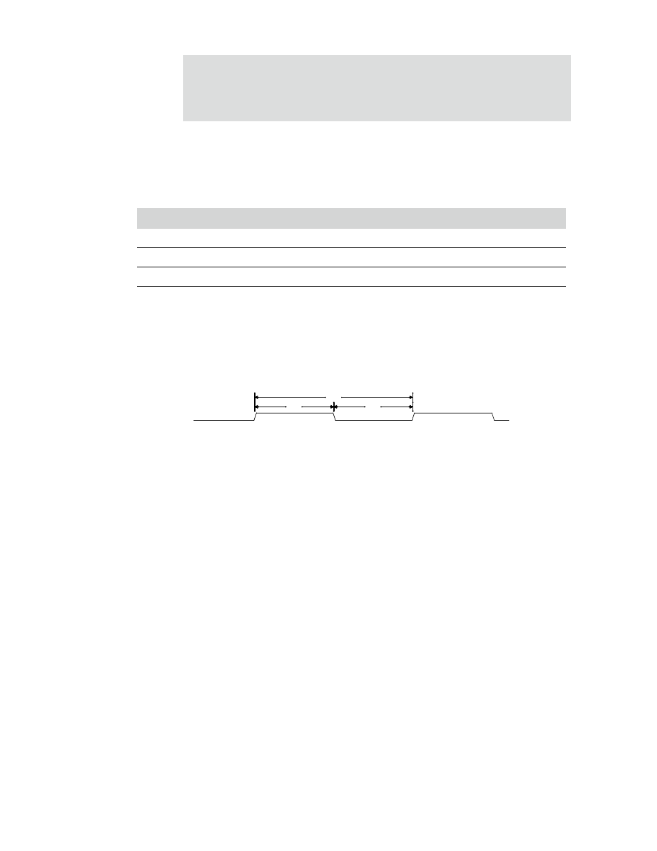
Table 483 describes the values shown in the system PLL bypass mode timing diagram
(Figure 148).
Note:
1
The system PLL can be bypassed. In this mode, the CPU clock speed is 1/2 of
x1_sys_osc
.
2
The minimum high/low time on system clock input pin when used with an external oscillator is 1.5nS.
Figure 148: System PLL bypass mode timing
Parm
Description
Min
Max
Unit
Notes
SC1
x1_sys_osc cycle time
2.5
5
ns
1
SC2
x1_sys_osc high time
(SC1/2) x 0.45
(SC1/2) x 0.55
ns
SC3
x1_sys_osc low time
(SC1/2) x 0.45
(SC1/2) x 0.55
ns
Table 483: System PLL bypass mode timing parameters
SC1
SC2
SC2
SC3
SC1
SC3
x1_sys_osc