Pci burst read from ns9750 timing, Pci burst write to ns9750 timing, The functional timing for – Digi NS9750 User Manual
Page 843: And the read data on, Trdy_n, devsel_n, Ad[31:0
w w w . d i g i e m b e d d e d . c o m
8 1 9
T i m i n g
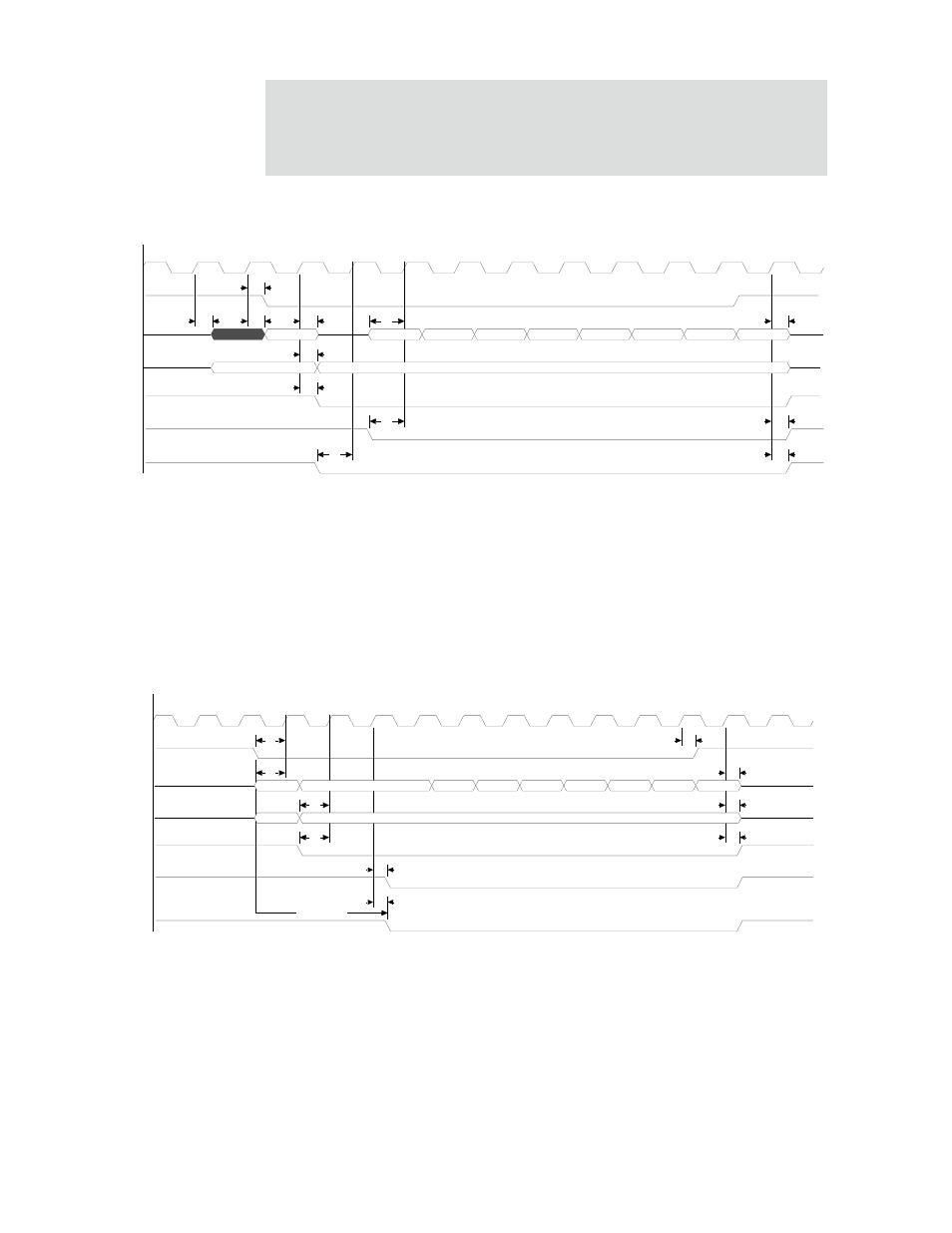
PCI burst read from NS9750 timing
Figure 123: PCI burst read from NS9750 timing
Note:
The functional timing for
trdy_n, devsel_n,
and the read data on
ad[31:0]
shows
the fastest possible response from the target.
PCI burst write to NS9750 timing
Figure 124: PCI burst write to NS9750 timing
P3
P2
P3
P2
P1
P1
P3
P2
P5
P1
P4
P1
byte enables
cmd
addr
data0
data1
data2
data3
data4
data5
data6
data7
pci_clk_in
frame_n
ad[31:0]
cbe_n[3:0]
irdy_n
trdy_n
devsel_n
3x pci_clk_in
P1
P1
P3
P2
P3
P2
P3
P2
P3
P2
byte enables
cmd
addr
data0
data1
data2
data3
data4
data5
data6
data7
pci_clk_in
frame_n
ad[31:0]
cbe_n[3:0]
irdy_n
trdy_n
devsel_n