Digi NS9750 User Manual
Page 154
S t a t i c m e m o r y c o n t r o l l e r
1 3 0
N S 9 7 5 0 H a r d w a r e R e f e r e n c e
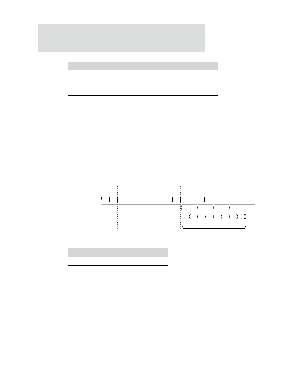
Figure 45 shows a burst of zero wait state reads with the length specified. Because
the length of the burst is known, the chip select can be held asserted during the
whole burst and generate the external transfers before the current AHB transfer has
completed. The first read requires five arbitration cycles; the three subsequent
sequential reads have zero AHB arbitration cycles added because the external
transfers are automatically generated. Table 57 provides the timing parameters.
Table 58 describes the transactions for Figure 45.
Figure 45: External memory 0 wait fixed length burst read timing diagram
T7
AHB address provided to memory controller.
T7-T8
AHB transaction processing.
T8-T11
Arbitration of AHB memory ports.
T11-T12
Static memory address, chip select, and control signals submitted to
static memory.
T12-T13
Read data returned from static memory. Data is provided to the AHB.
Timing parameter
Value
WAITRD
0
WAITOEN
0
WAITPAGE
N/A
WAITWR
N/A
Table 57: SRAM timing parameters
Cycle
Description
Table 56: External memory 2 0wait state reads
ADDR
DATAIN
A+C
CSCTSOUT_n
COEOUT_n
A
A+4
A+8
D(A)
D(A+4)
D(A+8)
D(A+C)
clk_out
T0
T1
T2
T3
T4
T5
T6
T7
T8