Ethernet interface – Digi NS9750 User Manual
Page 49
w w w . d i g i e m b e d d e d . c o m
2 5
N S 9 7 5 0 P i n o u t
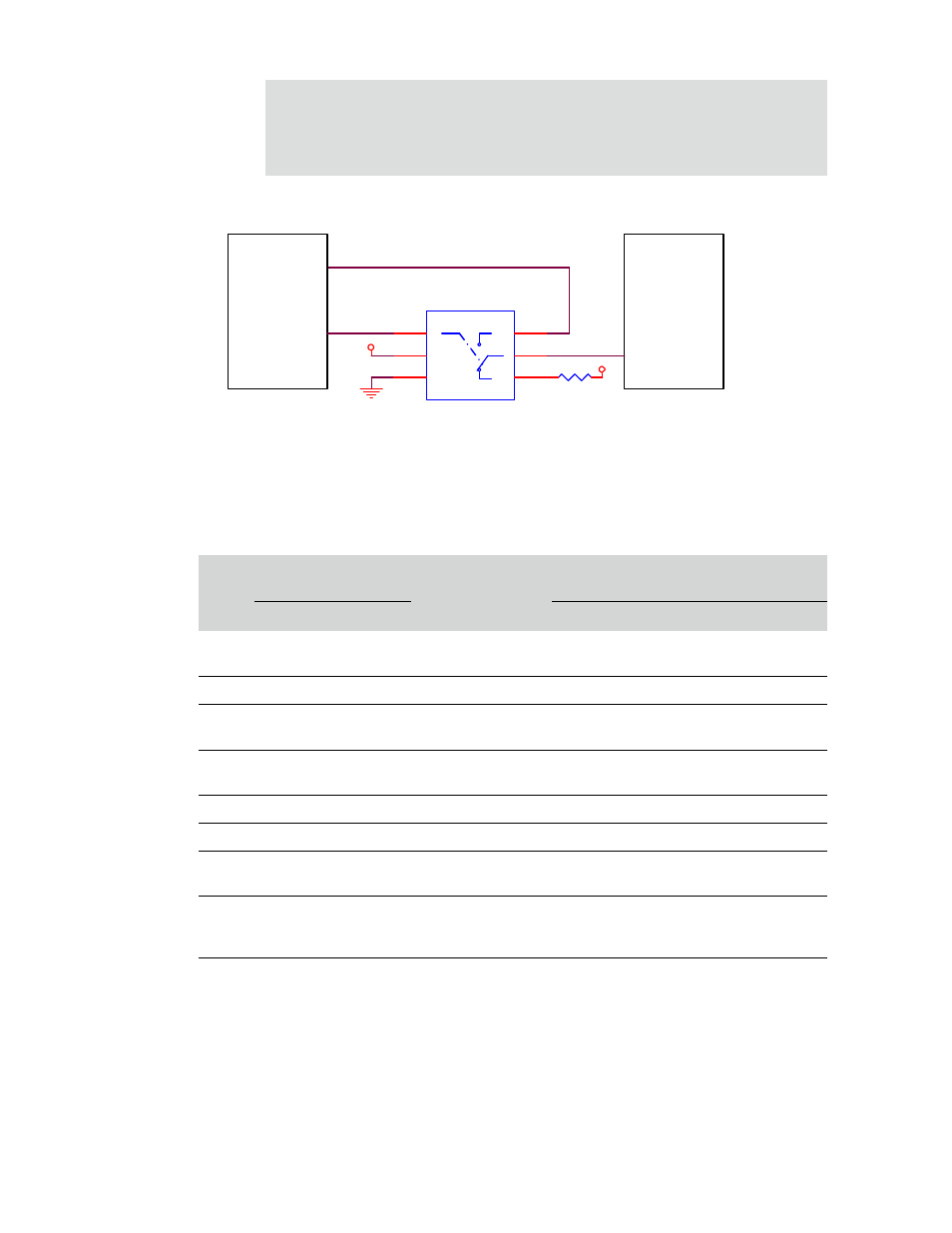
Figure 7: NS9750 clock enable configuration
Ethernet interface
3.3V
reset_done
clk_en[n]
SDRAM
NS9750
0 = B0 TO A
NC7SB3157
U1
4
3
1
2
5
6
A
B0
B1
GND
V+
S
2.4K
ohm
CKE
3.3V
Pin #
Signal name
U/D
OD
(mA)
I/O
Description
MII
RMII
MII
RMII
AB1
col
N/C
I
Collision
Pull low external to
NS9750
AA2
crs
crs_dv
I
Carrier sense
Carrier sense
AC1
enet_phy_i
nt_n
enet_phy_i
nt_n
U
I
Ethernet PHY
interrupt
Ethernet PHY
interrupt
AA3
mdc
mdc
4
O
MII management
interface clock
MII management
interface clock
AB2
mdio
mdio
U
2
I/O
MII management data
MII management data
T3
rx_clk
ref_clk
I
Receive clock
Reference clock
V2
rx_dv
N/C
I
Receive data valid
Pull low external to
NS9750
W1
rx_er
rx_er
I
Receive error
Optional signal; pull
low to NS9750 if not
used
V1
rxd[0]
rxd[0]
I
Receive data bit 0
Receive data bit 0
Table 5: Ethernet interface pinout