Internal pci arbiter timing, Pci burst write from ns9750 timing, The functional timing for – Digi NS9750 User Manual
Page 842: Figure 121: internal pci arbiter timing, Trdy_n, Devsel_n
P C I t i m i n g
8 1 8
N S 9 7 5 0 H a r d w a r e R e f e r e n c e
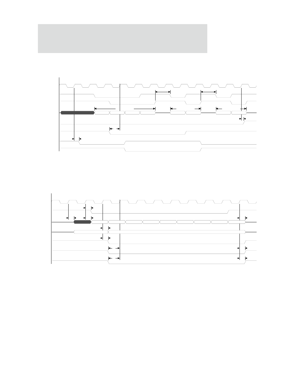
Internal PCI arbiter timing
Figure 121: Internal PCI arbiter timing
PCI burst write from NS9750 timing
Figure 122: PCI burst write from NS9750 timing
Note:
The functional timing for
trdy_n
and
devsel_n
shows the fastest possible
response from the target.
data0
addr
P1
P2
P3
Master 1 Cycle
Master 1 Cycle
Master 2 Cycle
Master 2 Cycle
Master 1 Cycle
Master 1 Cycle
Switch Master
Switch Master
addr
data1
data2
data0
addr
data0
pci_clk_in
frame_n
irdy_n
ad[31:0]
pci_arb_req_1_n
pci_arb_req_2_n
pci_arb_gnt_1_n
pci_arb_gnt_2_n
P3
P2
P3
P2
P1
P1
P5
P1
P4
P1
byte enables
cmd
addr
data0
data1
data2
data3
data4
data5
data6
data7
pci_clk_in
frame_n
ad[31:0]
cbe_n[3:0]
irdy_n
trdy_n
devsel_n