Digi NS9750 User Manual
Page 487
w w w . d i g i e m b e d d e d . c o m
4 6 3
P C I - t o - A H B B r i d g e
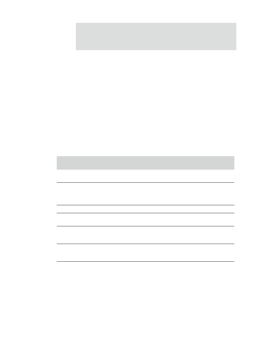
Notes:
1
The power controller is required only for applications that support hot-insertion
and hot-removal of the CardBus card. This requires additional components to
isolate NS9750 from CardBus.
2
The system must provide external pullup per PCI specification. CAD, C/BE, and
PAR do not require pullups.
3
Voltage detection signal optional for embedded system.
4
Pins not connected because internal resistors tie these to the appropriate state.
Configuring NS9750 for CardBus support
Although many CardBus signals are the same as those for the PCI bus, there are some
unique signals. Table 285 lists the new signals and indicates the PCI signals with which
they are multiplexed for NS9750.
PCI Signal
CardBus
Signal
CardBus type
Comments
INTA#
CINT#
Input
Cardbus interrupt pin. INTA2PCI in the PCI
Miscellaneous Support register must be 0.
INTB#
CCLKRUN#
Bidir
CardBus pin used to negotiate with the external
CardBus device before stopping the clock. Also
allows external CardBus device to request that the
clock be restarted.
INTC#
CSTSCHG
Input
CardBus status change interrupt signal.
GNT1#
CGNT#
Output
Grant to external CardBus device from NS9750’s
internal arbiter.
GNT2#
CVS1
Output
Voltage sense pin. Normally driven low by NS9750,
but toggled during interrogation of external CardBus
device to detect voltage requirements.
GNT3#
CVS2
Output
Voltage sense pin. Normally driven low by NS9750
but toggled during interrogation of external CardBus
device to detect voltage requirements.
REQ1#
CREQ#
Input
Request from external CardBus device to NS9750’s
internal arbiter.
Table 285: CardBus IO muxing