Cardbus miscellaneous support register, Register bit assignment, Table 279: cardbus miscellaneous support register – Digi NS9750 User Manual
Page 466: Volts can be supplied to the socket, Bits access mnemonic reset description
P C I b u s a r b i t e r
4 4 2
N S 9 7 5 0 H a r d w a r e R e f e r e n c e
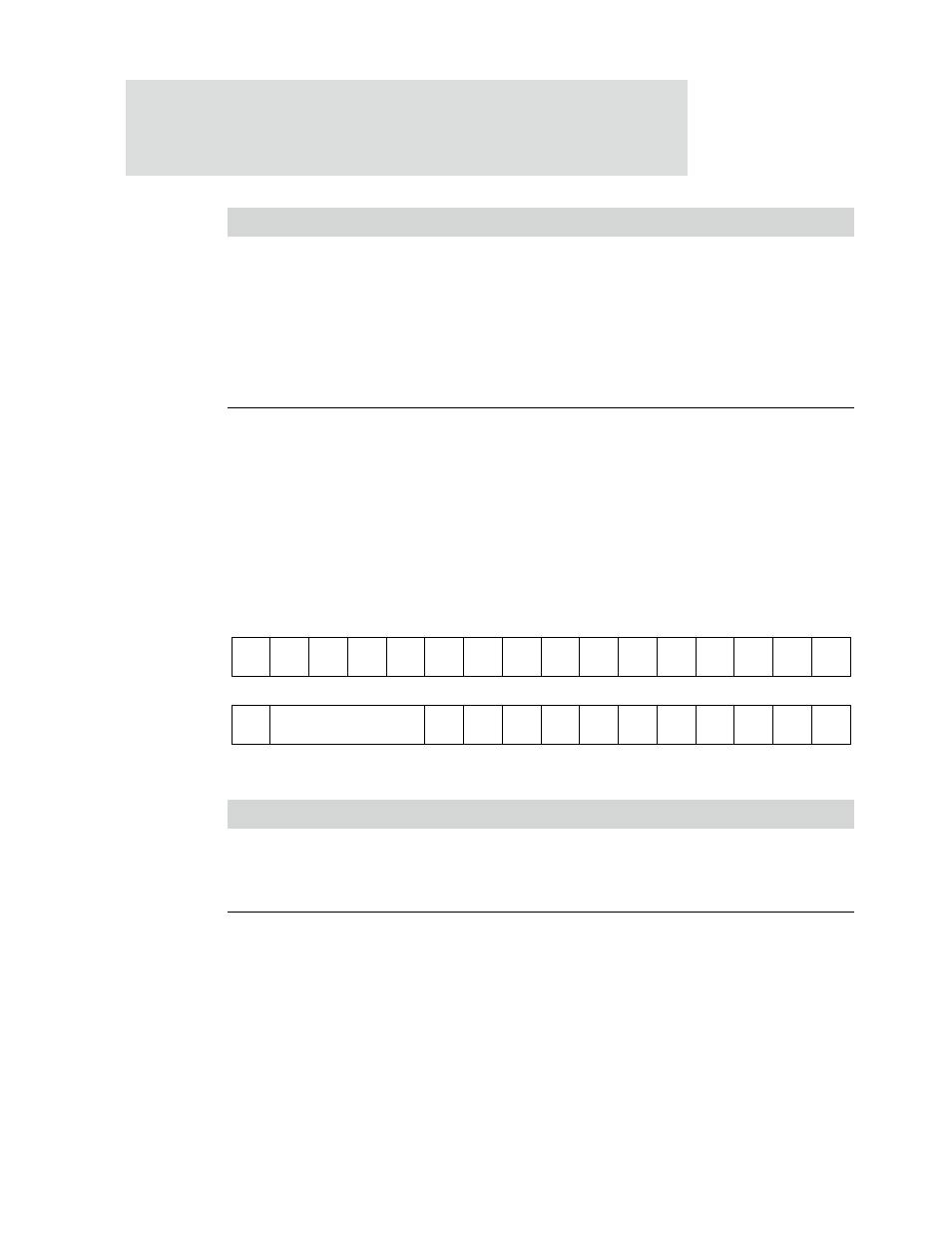
CardBus Miscellaneous Support register
Address: A030 004C
The CardBus Miscellaneous Support register is used for CardBus applications only, and
provides NS9750-specific CardBus control and status. (See the NS9750 Sample Driver
Configurations for examples of how this register is used.)
Register Bit Assignment
D00
R/W
PALT_EN
0
Enable AHB-to-PCI address translation for both
PCI memory and IO space
0
Do not translate AHB addresses. The same
addresses are used for both PCI and AHB.
1
Translate AHB addresses per the PALTxxVAL
fields in the PCI Bridge AHB-to-PCI Memory
Address Translate registers (see page 437 and
page 438) and the PCI Bridge AHB-to-PCI IO
Address Translate register (see page 439).
Bits
Access
Mnemonic
Reset
Description
D31
R/W
CMS_YV_SKT
0
Allows software to control the YV_SKT bit in
the CardBus Socket Present State register.
When set, indicates that
VCC=Y.Y
volts can be
supplied to the socket.
D30
R/W
CMS_XV_SKT
0
Allows software to control the XV_SKT bit in
the CardBus Socket Present State register.
When set, indicates that
VCC=X.X
volts can
be supplied to the socket.
Table 279: CardBus Miscellaneous Support register
Bits
Access
Mnemonic
Reset
Description
Table 278: PCI Bridge Address Translation Control register
REQ_
INTGT_
EN
Reserved
REQ_
INT
GATE
INTER-
RO-
GATE
Rsvd
CCLK
RUN_
EN
CVS2
CVS1
CCLK_
STOP_
NACK
CCLK_
STOP_
ACK
CCD2 CCD1
13
12
11
10
9
8
7
6
5
4
3
2
1
0
15
14
CMS_
CCD1
31
29
28
27
26
25
24
23
22
21
20
19
18
17
16
30
CMS_
V3
SKT
CMS_
V5
SKT
CMS_
YV_
CARD
Rsvd
CMS_
XV
CARD
CMS_
V3_
CARD
CMS_
V5
CARD
CMS_
BAD_
VCC
CMS_
DATA_
LOST
CMS_
NOTA_
CARD
CMS_
CB_
CARD
CMS_
CARD_
16
CMS_
PWR_
CYC
CMS_
CCD2
CMS_
YV_
SKT
CMS_
XV_
SKT