Lcd input clock timing – Digi NS9750 User Manual
Page 862
C l o c k t i m i n g
8 3 8
N S 9 7 5 0 H a r d w a r e R e f e r e n c e
LCD input clock timing
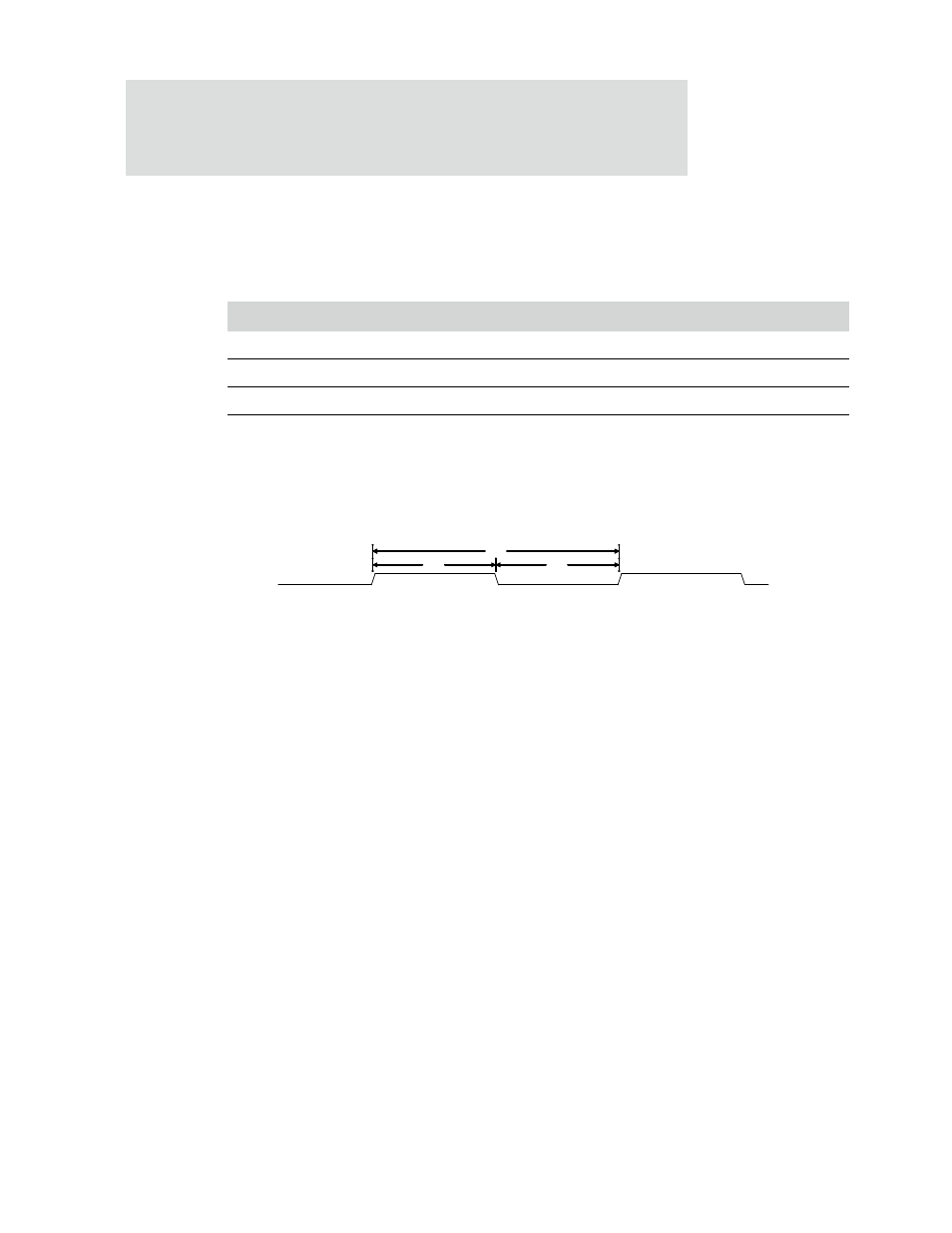
Table 482 describes the values shown in the LCD input clock timing diagram
(Figure 147).
Note:
1
The clock rate supplied on
lcdclk
is twice the actual LCD clock rate.
Figure 147: LCD input clock timing
Parm
Description
Min
Max
Unit
Notes
LC1
lcdclk cycle time
6.25
ns
1
LC2
lcdclk high time
(LC1/2) x 0.4
(LC1/2) x 0.6
ns
LC3
lcdclk low time
(LC1/2) x 0.4
(LC1/2) x 0.6
ns
Table 482: LCD input clock timing parameters
LC2
LC1
LC2
LC3
LC1
LC3
lcdclk