Fifo status and control registers, Register bit assignment – Digi NS9750 User Manual
Page 805
w w w . d i g i e m b e d d e d . c o m
7 8 1
U S B C o n t r o l l e r M o d u l e
Register bit assignment
FIFO Status and Control registers
Address: 9010 3100 / 3108 / 3110 / 3118 / 3120 / 3128 / 3130 / 3138 / 3140 / 3148 / 3150 / 3158 /
3160
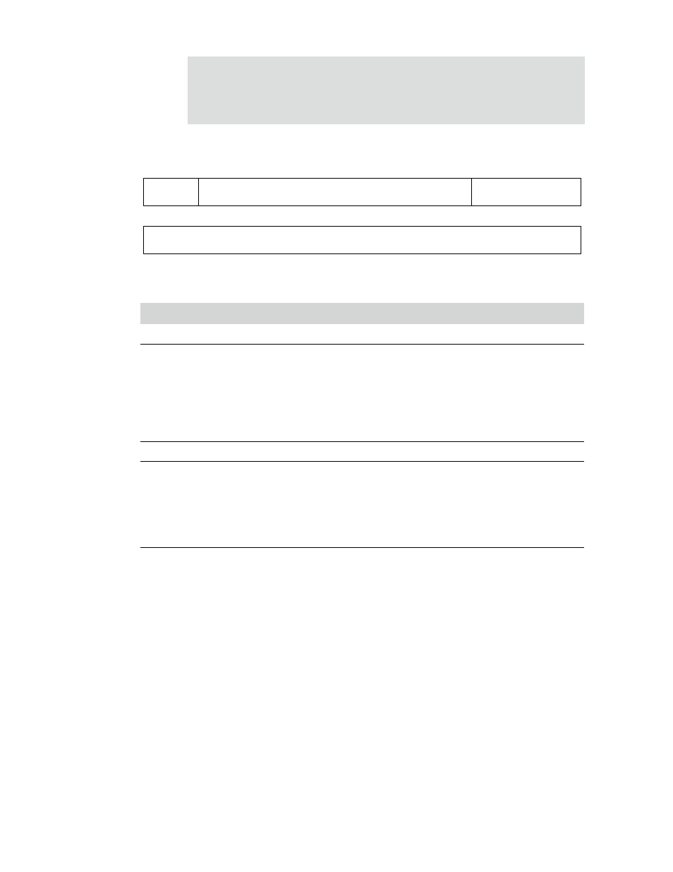
The FIFO Status and Control registers contain additional status and control
information for the device block FIFOs. There are 13 of these registers in the USB
module, one for each non-control endpoint and the two required for the bidirectional
endpoint.
Bits
Access
Mnemonic
Reset
Description
D31:30
N/A
Not used
0x0
Always read as 0x0.
D29:20
R/W
MAX
0x040
Indicates the maximum packet size supported by the
associated USB device endpoint. This value should be set
to the same value as the maximum packet size (see
page 766) in the Endpoint Descriptor register.
Note:
This field does not apply for FIFO #2 as that
FIFO is dedicated to the IN direction of the
control endpoint.
D19:16
N/A
Not used
0x00
Always read as 0x00.
D15:00
R
COUNT
0x0000
Indicates the number of error-free packets sent by the USB
device module (USB-IN transactions) with the current
DMA buffer descriptor for the associated FIFO.
Note:
This field does not apply for FIFO #1 as that
FIFO is dedicated to the OUT direction of the
control endpoint.
Table 458: FIFO Packet Control registers
13
12
11
10
9
8
7
6
5
4
3
2
1
0
15
14
31
29
28
27
26
25
24
23
22
21
20
19
18
17
16
30
MAX
COUNT
Not
used
Not used