Digi NS9750 User Manual
Page 828
M e m o r y t i m i n g
8 0 4
N S 9 7 5 0 H a r d w a r e R e f e r e n c e
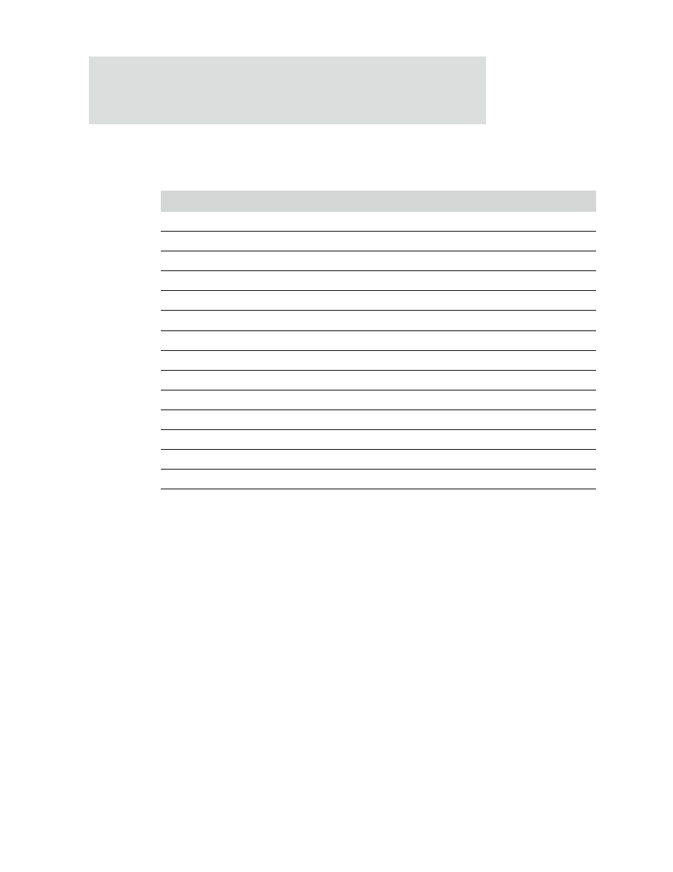
Table 468 describes the values shown in the SRAM timing diagrams (Figure 113
through Figure 118).
Notes:
1
The (CPU clock out / 2) signal is for reference only.
2
Only one of the four
dy_cs_n
signals is used. The diagrams show the active low configuration, which can be
reversed (active high) with the PC field.
3
Use this formula to calculate the length of the st_cs_n signal:
Tacc + board delay + (optional buffer delays, both address out and data in) + 10ns
Parm
Description
Min
Max
Unit
Notes
M15
clock high to data out valid
-2
+2
ns
M16
data out hold time from clock high
-2
+2
ns
M17
clock high to address valid
-2
+2
ns
M18
address hold time from clock high
-2
+2
ns
M19
clock high to st_cs_n low
-2
+2
ns
2
M20
clock high to st_cs_n high
-2
+2
ns
2
M21
clock high to we_n low
-2
+2
ns
M22
clock high to we_n high
-2
+2
ns
M23
clock high to byte_lanes low
-2
+2
ns
M24
clock high to byte_lanes high
-2
+2
ns
M25
data input setup time to rising clk
10
ns
M26
data input hold time to rising clk
0
ns
M27
clock high to oe_n low
-2
+2
ns
M28
clock high to oe_n high
-2
+2
ns
Table 468: SRAM timing parameters