Register bit assignment – Digi NS9750 User Manual
Page 521
w w w . d i g i e m b e d d e d . c o m
4 9 7
B B u s B r i d g e
Register bit assignment
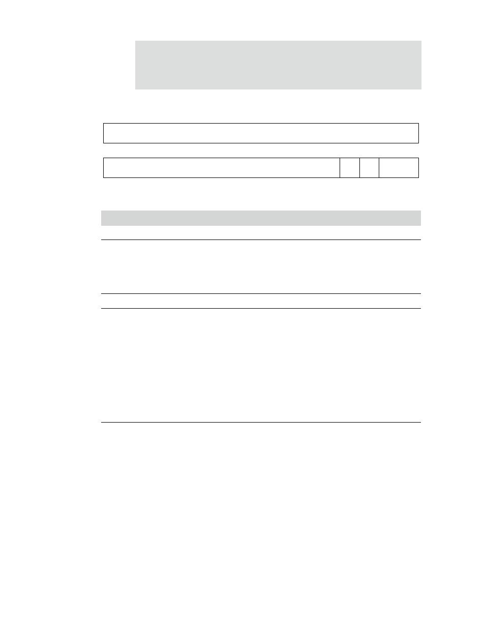
Bits
Access
Mnemonic
Reset
Description
D31:04
R/W
Not used
0
Always set to 0.
D03
R/W
POL
0
Chip select polarity
Defines the polarity of the memory interface chip select
signal (
stcsout[n]_n
) connected to the external peripheral.
0
Defines an active high signal
1
Defines an active low signal
D02
R/W
Not used
0
Always set to 0.
D01:00
R/W
SEL
0
Chip select selection
Defines which of the four memory interface chip select
signals (
stcsout[n]_n
) is connected to the external
peripheral.
Value
Chip select
0
CS[0]
1
CS[1]
2
CS[2]
3
CS[3]
Note:This field is not used for memory-to-memory
transfers.
Table 299: DMA Peripheral Chip Select register
13
12
11
10
9
8
7
6
5
4
3
2
1
0
15
14
31
29
28
27
26
25
24
23
22
21
20
19
18
17
16
30
Not used
Not used
POL
Not
used
SEL