Pci burst read to ns9750 timing, Pci clock timing, The functional timing for valid read data on – Digi NS9750 User Manual
Page 844: Ad[31:0
P C I t i m i n g
8 2 0
N S 9 7 5 0 H a r d w a r e R e f e r e n c e
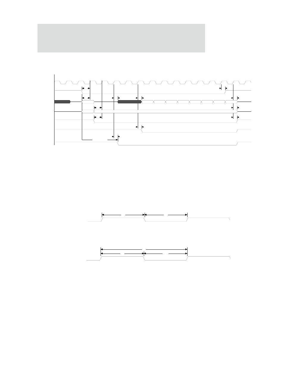
PCI burst read to NS9750 timing
Figure 125: PCI burst read to NS9750 timing
Note:
The functional timing for valid read data on
ad[31:0]
is just an example. The
actual response time will depend on when the PCI bridge gets access to
the AHB bus internal to NS9750.
PCI clock timing
Figure 126: pci_clock_out timing
Figure 127: pci_clk_in timing
3x pci_clk_in
P1
P1
P3
P2
P3
P2
P5
P1
P4
P2
P3
P2
byte enables
cmd
addr
data0
data1
data2
data3
data4
data5
data6
data7
N t
pci_clk_in
frame_n
ad[31:0]
cbe_n[3:0]
irdy_n
trdy_n
devsel_n
P7
P7
P6
P6
pci_clk_out
P10
P8
P10
P9
P9
P8
pci_clk_in