Jtag timing – Digi NS9750 User Manual
Page 860
J T A G t i m i n g
8 3 6
N S 9 7 5 0 H a r d w a r e R e f e r e n c e
JTAG timing
Note:
All AC characteristics are measured with 10pF, unless otherwise noted.
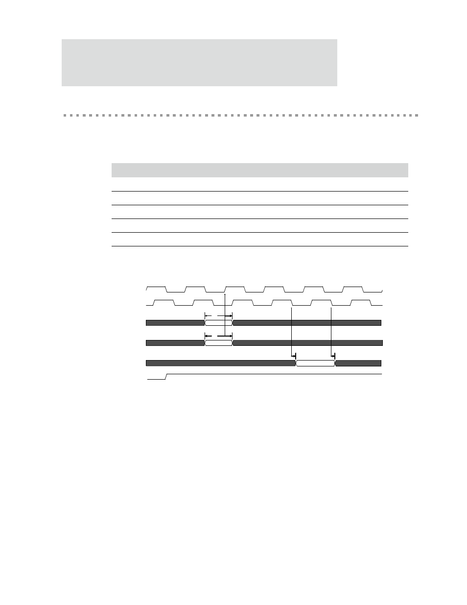
Table 480 describes the values shown in the JTAG timing diagram (Figure 145).
Figure 145: JTAG timing
Notes:
1
Maximum tck rate is 10 MHz.
2
rtck_out
is an asynchronous output, driven off of the CPU clock.
3
trst_n
is an asynchronous input.
Parm
Description
Min
Max
Unit
J1
tms (input) setup to tck rising
5
ns
J2
tms (input) hold to tck rising
2
ns
J3
tdi (input) setup to tck rising
5
ns
J4
tdi (input) hold to tck rising
2
ns
J5
tdo (output) to tck falling
2.5
10
ns
Table 480: JTAG timing parameters
J1
J2
J3
J4
J5
J5
tck
rtck_out
tms
tdi
tdo
trst_n