Digi NS9750 User Manual
Page 156
S t a t i c m e m o r y c o n t r o l l e r
1 3 2
N S 9 7 5 0 H a r d w a r e R e f e r e n c e
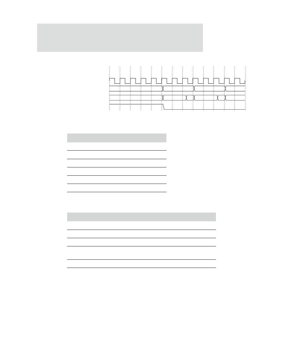
Figure 46: External memory 2 wait states fixed length burst read timing diagram
Timing parameter
Value
WAITRD
2
WAITOEN
0
WAITPAGE
N/A
WAITWR
N/A
WAITWEN
N/A
WAITTURN
N/A
Table 59: SRAM timing diagrams
Cycle
Description
T0
AHB address provided to memory controller.
T0-T1
AHB transaction processing.
T1-T4
Arbitration of memory ports.
T4-T5
Static memory address, chip select, and control signals submitted to
static memory.
T5-T6
Read wait state 1.
T6-T7
Read wait state 2.
Table 60: External memory 2 wait states fixed length burst read
ADDR
DATAIN
A+8
SCTSOUT_n
COEOUT_n
A
A+4
D(A)
D(A+4)
clk_out
T0
T1
T2
T3
T4
T5
T6
T7
T12
T10
T11
T8
T9