Register bit assignment – Digi NS9750 User Manual
Page 332
S y s t e m c o n f i g u r a t i o n r e g i s t e r s
3 0 8
N S 9 7 5 0 H a r d w a r e R e f e r e n c e
Register bit assignment
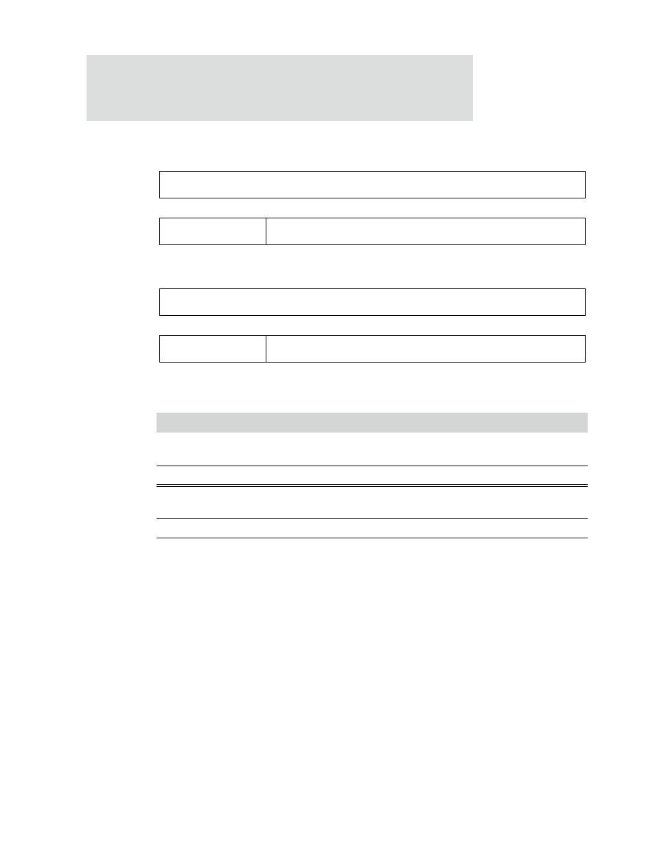
System Memory Chip Select 1 Static Memory Base and Mask registers
Address: A09001F8 / 01FC
These control registers set the base and mask for system memory chip select 1, with
a minimum size of 4K. The powerup default settings produce a memory range of
0x5000 0000 — 0x5FFF FFFF
.
Bits
Access
Mnemonic
Reset
Description
D31:12
R/W
CS0B
0x40000
Chip select 0 base
Base address for chip select 0 (static).
D11:00
N/A
Reserved
N/A
N/A
D31:12
R/W
CS0M
0xF0000
Chip select 0 mask
Mask or size for chip select 0 (static).
D11:00
N/A
Reserved
N/A
N/A
Table 195: System Memory Chip Select 0 Static Memory Base & Mask registers
13
12
11
10
9
8
7
6
5
4
3
2
1
0
15
14
31
29
28
27
26
25
24
23
22
21
20
19
18
17
16
30
Chip select 0 base (CS0B)
Reserved
Chip select 0 base (CS0B)
13
12
11
10
9
8
7
6
5
4
3
2
1
0
15
14
31
29
28
27
26
25
24
23
22
21
20
19
18
17
16
30
Chip select 0 mask (CS0M)
Reserved
Chip select 0 mask (CS0M)