Digi NS9750 User Manual
Page 46
P i n o u t a n d s i g n a l d e s c r i p t i o n s
2 2
N S 9 7 5 0 H a r d w a r e R e f e r e n c e
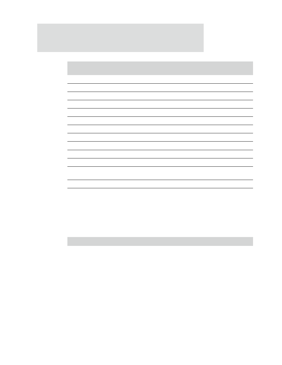
System Memory interface signals
Table 4 describes System Memory interface signals in more detail. All signals are
internal to the chip.
A8
dy_cs_n[0]
8
O
SDRAM chip select signal
B8
dy_cs_n[1]
8
O
SDRAM chip select signal
A6
dy_cs_n[2]
8
O
SDRAM chip select signal
C7
dy_cs_n[3]
8
O
SDRAM chip select signal
C6
st_oe_n
8
O
Static memory output enable
D6
ras_n
8
O
SDRAM row address strobe
H1
dy_pwr_n
8
O
SyncFlash power down
B10
st_cs_n[0]
8
O
Static memory chip select signal
C10
st_cs_n[1]
8
O
Static memory chip select signal
B9
st_cs_n[2]
8
O
Static memory chip select signal
C9
st_cs_n[3]
8
O
Static memory chip select signal
B6
we_n
8
O
SDRAM write enable. Used for static and
SDRAM devices.
J3
ta_strb
U
I
Slow peripheral transfer acknowledge
Pin #
Signal Name
U/D
OD
(mA)
I/O
Description
Table 3: System Memory interface pinout
Name
I/O
Description
addr[27:0]
O
Address output. Used for both static and SDRAM devices. SDRAM
memories use bits [14:0]; static memories use bits [25:0].
Table 4: System Memory interface signal descriptions