Mii management configuration register, Register bit assignment – Digi NS9750 User Manual
Page 383
w w w . d i g i e m b e d d e d . c o m
3 5 9
E t h e r n e t C o m m u n i c a t i o n M o d u l e
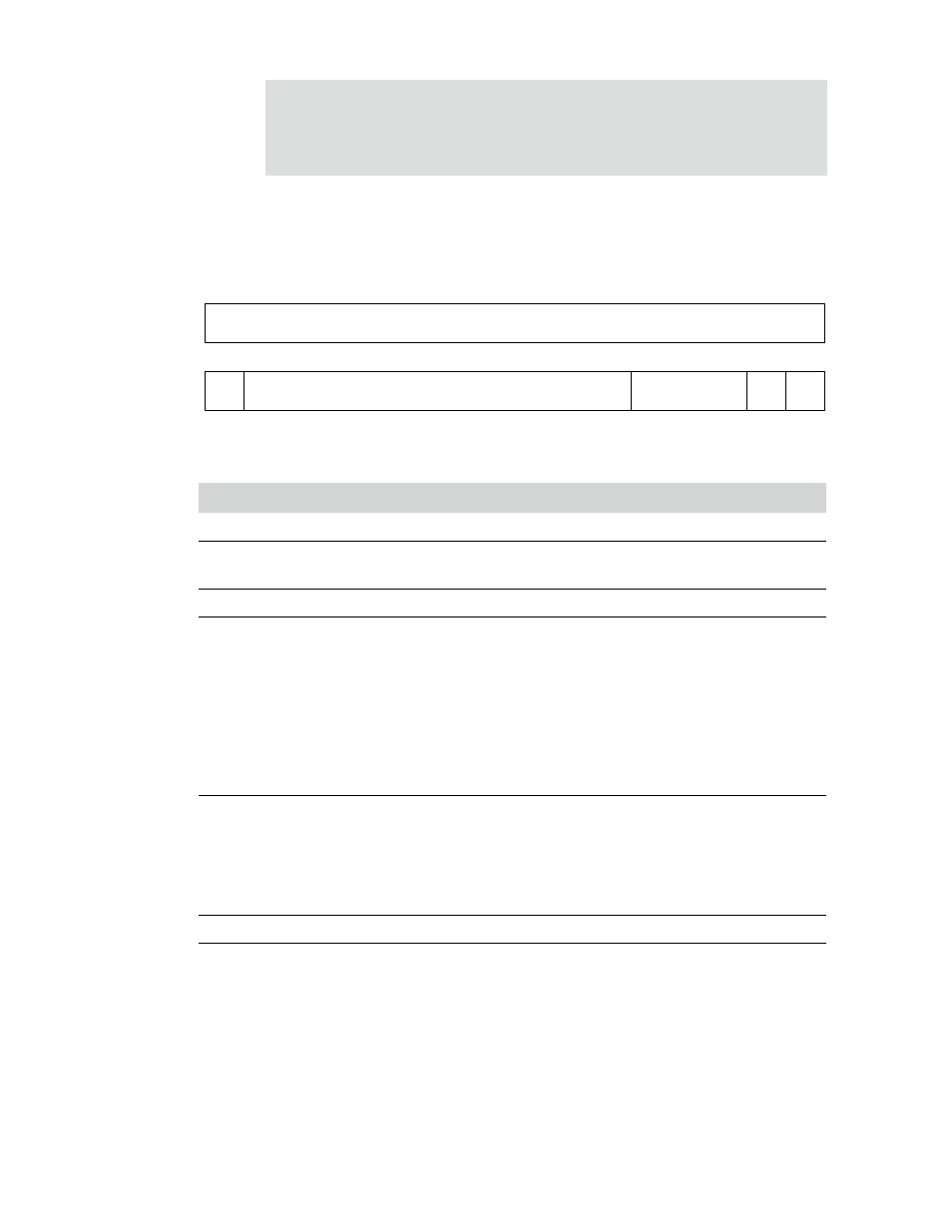
MII Management Configuration register
Address: A060 0420
Register bit assignment
Bits
Access
Mnemonic
Reset
Description
D31:16
N/A
Reserved
N/A
N/A
D15
R/W
RMIIM
0
Reset MII management block
Set this bit to 1 to reset the MII Management module.
D14:05
N/A
Reserved
N/A
N/A
D04:02
R/W
CLKS
0x0
Clock select
Used by the clock divide logic in creating the MII
management clock, which (per the IEEE 802.3u
standard) can be no faster than 2.5 MHz.
Note:
Some PHYs support clock rates up to 12.5
MHz.
The AHB bus clock is used as the input to the clock
divide logic. "Clocks field settings," on page 360,
shows the settings that are supported.
D01
R/W
SPRE
0
Suppress preamble
0
Causes normal cycles to be performed
1
Causes the MII Management module to perform
read/write cycles without the 32-bit preamble
field. (Preamble suppression is supported by
some PHYs.)
D00
R/W
Not used
0
Always write to 0.
Table 218: MII Management Configuration register
Reserved
Not
used
13
12
11
10
9
8
7
6
5
4
3
2
1
0
15
14
31
29
28
27
26
25
24
23
22
21
20
19
18
17
16
30
Reserved
CLKS
SPRE
RMIIM