Lcdtiming3, Lcdupbase and lcdlpbase, Lcdtiming3 controls whether the line-end signal – Digi NS9750 User Manual
Page 611: Is enabled. when enabled, a positive pulse, four, Periods wide, is output on
w w w . d i g i e m b e d d e d . c o m
5 8 7
L C D C o n t r o l l e r
LCDTiming3
Address: A080 000C
LCDTiming3 controls whether the line-end signal,
CLLE
, is enabled. When enabled, a
positive pulse, four
CLCDCLK
periods wide, is output on
CLLE
after a programmable
delay from the last pixel of each display line. If the line-end signal is disabled, it is
held permanently low.
Register bit assignment
LCDUPBASE and LCDLPBASE
Address: A080 0010 and A080 0014
LCDUPBASE and LCDLPBASE are the DMA base address registers, and program the base
address of the frame buffer.
Bits
Access
Mnemonic
Reset
Description
D31:17
N/A
Reserved
N/A
N/A
D16
R/W
LEE
0x0
LCD line-end enable
0
CLLE
disabled (held low)
1
CLLE
signal active
D15:07
N/A
Reserved
N/A
N/A
D06:00
R/W
LED 0x00
Line-end signal delay
Line-end signal delay from the rising edge of the last
panel clock (
CLCP
). Program this field with number of
CLCDCLK
clock periods
minus 1.
Table 354: LCDTiming3 register
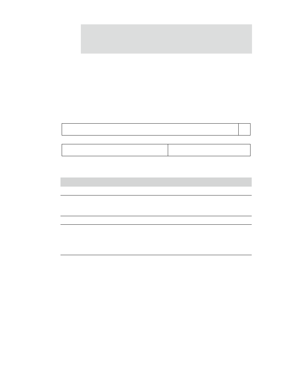
LED
13
12
11
10
9
8
7
6
5
4
3
2
1
0
15
14
Reserved
31
29
28
27
26
25
24
23
22
21
20
19
18
17
16
30
Reserved
LEE