Configuration register, C bus clock timing is programmable by the, Value – Digi NS9750 User Manual
Page 576
I 2 C r e g i s t e r s
5 5 2
N S 9 7 5 0 H a r d w a r e R e f e r e n c e
Configuration register
Address: 9050 000C
The Configuration register controls the timing on the I
2
C bus. This register also
controls the external interrupt indication, which can be disabled.
The I
2
C bus clock timing is programmable by the
scl_ref
value (
D08:00
). The timing
parameter for standard mode is as follows:
I
2
C_bus_clock = clk / ((CLREF*2) + 4 + scl_delay)
clk = cpu_clk/4
Note:
In noisy environments and fast-mode transmission, spike filtering can be
applied to the received I
2
C data and clock signal. The spike filter
evaluates the incoming signal and suppresses spikes. The maximum length
of the suppressed spikes can be specified in the spike filter width field of
the Configuration register (see page 553).
The timing parameter for fast-mode is as follows:
I
2
C_bus_clock = (4 / 3) x (clk / ((CLREF*2) + 4 + scl_delay))
scl_delay
is influenced by the SCL rise time.
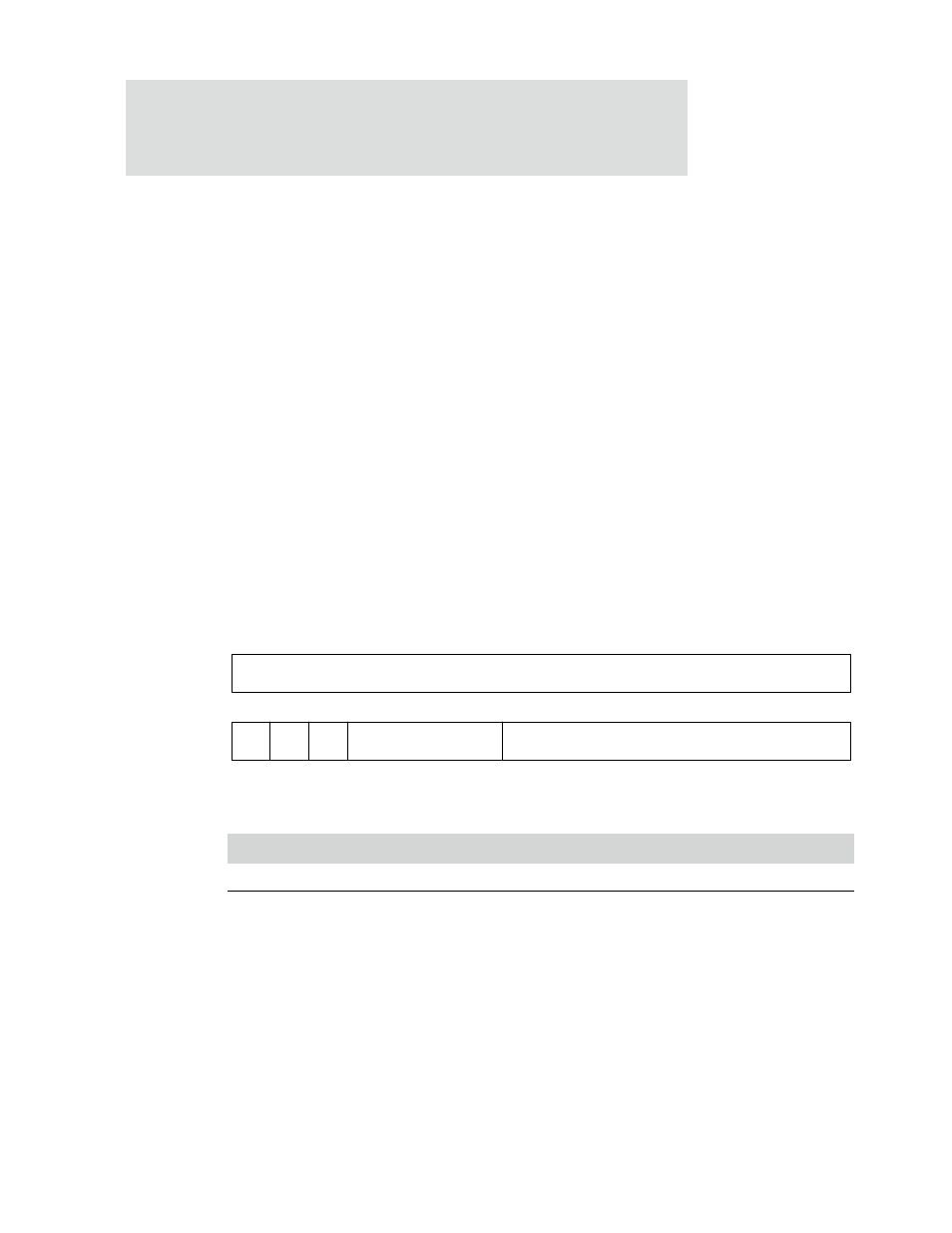
Register bit assignment
Bits
Access
Mnemonic
Reset
Description
D31:16
N/A
Reserved
N/A
N/A
D15
R/W
IRQD
0
Mask the interrupt to the ARM CPU (
irq_dis
)
Must be set to 0.
Table 341: Configuration register
13
12
11
10
9
8
7
6
5
4
3
2
1
0
15
14
31
29
28
27
26
25
24
23
22
21
20
19
18
17
16
30
Reserved
CLREF
IRQD
TMDE VSCD
SFW
s