Digi NS9750 User Manual
Page 163
w w w . d i g i e m b e d d e d . c o m
1 3 9
M e m o r y C o n t r o l l e r
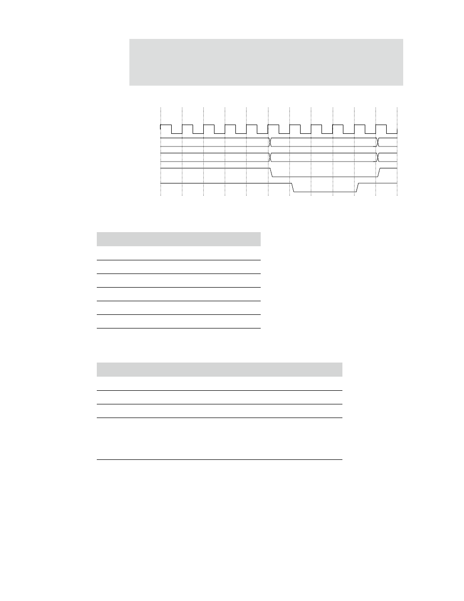
Figure 50: External memory 2 wait state write timing diagram
Timing parameter
Value
WAITRD
N/A
WAITOEN
N/A
WAITPAGE
N/A
WAITWR
2
WAITWEN
0
WAITTURN
N/A
Table 67: Static memory timing parameters
Cycle
Description
T0
AHB address provided to memory controller.
T0-T1
AHB transaction processing.
T1-T4
Arbitration of AHB memory ports.
T4-T5
Static memory transfer 0, address, chip select, and control signals
submitted to static memory.
Write data is read from the AHB memory port.
Write enable inactive.
T5-T6
Write enable taken active.
Write data submitted to static memory.
Table 68: External memory 2 wait state write
ADDR
DATAOUT
A
STCSOUT_n
D(A)
WEOUT_n
clk_out
T0
T1
T2
T3
T4
T5
T6
T7
T8
T9
T10