Digi NS9750 User Manual
Page 50
P i n o u t a n d s i g n a l d e s c r i p t i o n s
2 6
N S 9 7 5 0 H a r d w a r e R e f e r e n c e
Clock generation/system pins
U3
rxd[1]
rxd[1]
I
Receive data bit 1
Receive data bit 1
U2
rxd[2]
N/C
I
Receive data bit 2
Pull low external to
NS9750
U1
rxd[3]
N/C
I
Receive data bit 3
Pull low external to
NS9750
V3
tx_clk
N/C
I
Transmit clock
Pull low external to
NS9750
AA1
tx_en
tx_en
2
O
Transmit enable
Transmit enable
Y3
tx_er
N/C
2
O
Transmit error
N/A
Y2
txd[0]
txd[0]
2
O
Transmit data bit 0
Transmit data bit 0
W3
txd[1]
txd[1]
2
O
Transmit data bit 1
Transmit data bit 1
Y1
txd[2]
N/C
2
O
Transmit data bit 2
N/A
W2
txd[3]
N/C
2
O
Transmit data bit 3
N/A
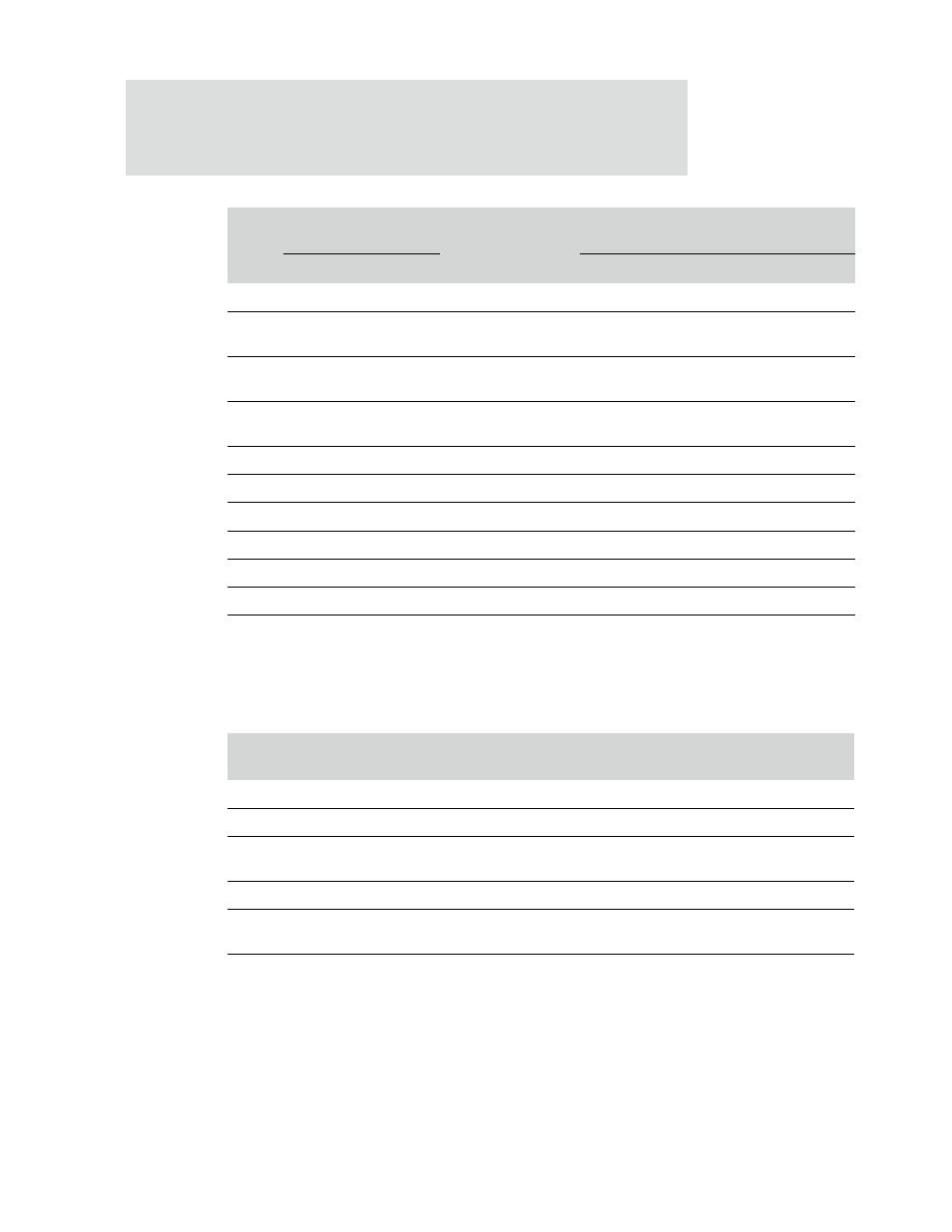
Pin #
Signal name
U/D
OD
(mA)
I/O
Description
MII
RMII
MII
RMII
Table 5: Ethernet interface pinout
Pin #
Signal name
U/D
OD
(mA)
I/O
Description
C8
x1_sys_osc
I
System clock crystal oscillator circuit input
B7
x2_sys_osc
O
System clock crystal oscillator circuit output
D9
x1_usb_osc
I
USB clock crystal oscillator circuit input.
(Connect to GND if USB is not used.)
A7
x2_usb_osc
O
USB clock crystal oscillator circuit output
AC21
reset_done
U
2
I/O
CPU is enabled once the boot program is loaded.
Reset_done is set to 1.
H25
reset_n
U
I
System reset input signal
Table 6: Clock generation and system pin pinout