Digi NS9750 User Manual
Page 193
w w w . d i g i e m b e d d e d . c o m
1 6 9
M e m o r y C o n t r o l l e r
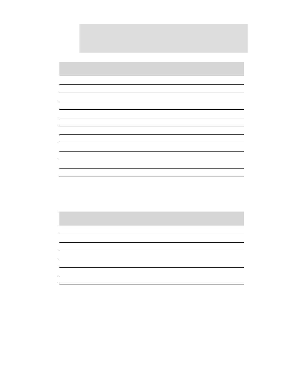
Table 97 shows the outputs from the memory controller and the corresponding inputs
to the 64M SDRAM (8Mx16, pins 13 and 14 used as bank selects).
11
11
23
-
10
10/AP
22
AP
9
9
21
-
8
8
20
-
7
7
19
9
6
6
18
8
5
5
17
7
4
4
16
6
3
3
15
5
2
2
14
4
1
1
13
3
0
0
12
2
Output address
(
ADDROUT
)
Memory device
connections
AHB address to row
address
AHB address to
column address
14
BA1
11
11
13
BA0
12
12
12
-
-
-
11
11
24
-
10
10/AP
23
AP
9
9
22
-
8
8
21
10
7
7
20
9
Table 97: Address mapping for 128 SDRAM (8Mx16, RBC)
Output address
(
ADDROUT
)
Memory device
connections
AHB address to row
address
AHB address to
column address
Table 96: Address mapping for 128M SDRAM (4Mx32, RBC)