Address decoding – Digi NS9750 User Manual
Page 285
w w w . d i g i e m b e d d e d . c o m
2 6 1
S y s t e m C o n t r o l M o d u l e
Address decoding
A central address decoder provides a select signal —
hsel_x
— for each slave on the bus.
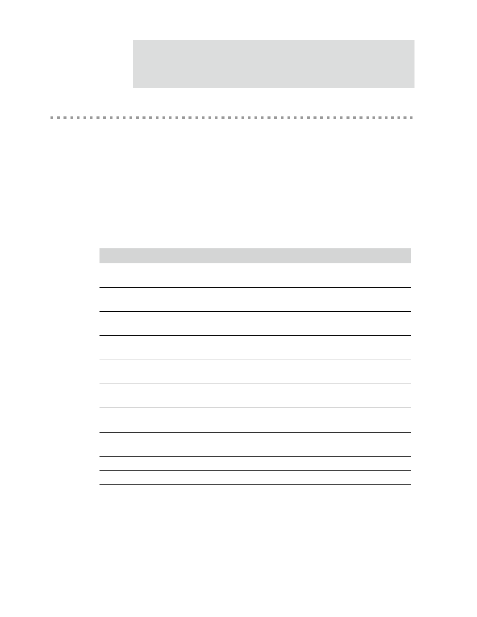
Table 166 shows how the system memory address is set up to allow access to the
internal and external resources on the system bus. Note that the external memory
chip select ranges can be reset after powerup. The table shows the default powerup
values; you can change the ranges by writing to the BASE and MASK registers (see
"System Memory Chip Select 0 Dynamic Memory Base and Mask registers" on page 303
through "System Memory Chip Select 3 Dynamic Memory Base and Mask registers" on
page 306 for more information).
See the BBus bridge chapter for information about BBus peripheral address decoding.
Address range
Size
System functions
0x0000 0000 – 0x0FFF FFFF
256 MB
System memory chip select 4
Dynamic memory (default)
0x1000 0000 – 0x1FFF FFFF
256 MB
System memory chip select 5
Dynamic memory (default)
0x2000 0000 – 0x2FFF FFFF
256 MB
System memory chip select 6
Dynamic memory (default)
0x3000 0000 – 0x3FFF FFFF
256 MB
System memory chip select 7
Dynamic memory (default)
0x4000 0000 – 0x4FFF FFFF
256 MB
System memory chip select 0
Static memory (default)
0x5000 0000 – 0x5FFF FFFF
256 MB
System memory chip select 1
Static memory (default)
0x6000 0000 – 0x6FFF FFFF
256 MB
System memory chip select 2
Static memory (default)
0x7000 0000 – 0x7FFF FFFF
256 MB
System memory chip select 3
Static memory (default)
0x8000 0000 – 0x8FFF FFFF
256 MB
PCI memory
0x9000 0000 – 0x9FFF FFFF
256 MB
BBus memory
0xA000 0000 – 0xA00F FFFF
1 MB
PCI IO
Table 166: System address map