Figure 6: sdram clock termination – Digi NS9750 User Manual
Page 48
P i n o u t a n d s i g n a l d e s c r i p t i o n s
2 4
N S 9 7 5 0 H a r d w a r e R e f e r e n c e
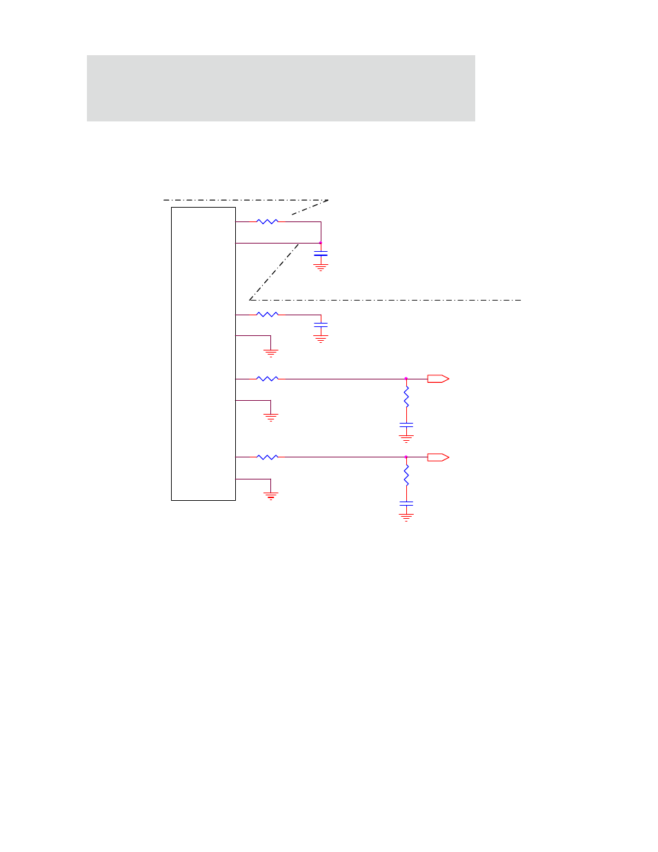
Figure 6 shows NS9750 SDRAM clock termination.
Figure 6: SDRAM clock termination
C3
clk_in[0]
clk_out[0]
C4
Always GND
Always GND
NS9750
clk_in[1]
Unused clk_out's are
terminated only
All series termination resistors
must be placed close to driver
Always connect clk_out[0]
to clk_in[0] using series
termination. Must not
drive any SDRAM loads.
Data in from SDRAMs is
sampled on the rising
edge of this clock.
Always GND
clk_in[2]
clk_out[3]
Address. Data, & Commands
are sampled by SDRAMs on
the rising edge of these
clocks.
clk_out[2]
CLK_IN[0]
SDRAM Bank B
SDRAM Banks have AC
Termination placed
at end of traces
clk_in[3]
SDRAM Bank A
UNUSED_CLK
clk_out[1]
SDRAM_CLK[3]
R3
R1
SDRAM_CLK[2]
This trace can be a loop 2 to 3 inches in length.
Read Data clock will be delayed 180pS/per inch.