Digi NS9750 User Manual
Page 159
w w w . d i g i e m b e d d e d . c o m
1 3 5
M e m o r y C o n t r o l l e r
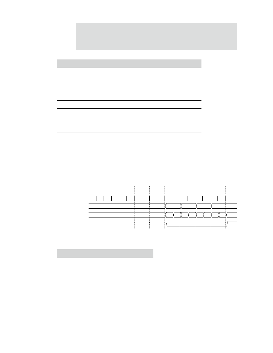
Figure 48 shows a 32-bit read from an 8-bit page mode ROM device, causing four burst
reads to be performed. A total of eight AHB wait states are added during this
transfer, five AHB arbitration cycles and then one for each of the subsequent reads.
WAITRD
and
WAITPAGE
are 0. Table 63 provides the timing parameters. Table 64
describes the transactions for Figure 48.
Figure 48: External memory 32-bit burst read from 8-bit memory timing diagram
T8-T9
Read page mode wait state 1.
T9-T10
Read data 1 returned from the static memory.
Read data 1 is provided to the AHB.
Static memory transfer 2, address, chip select, and control signals
submitted to static memory.
T10-T11
Read page mode wait state 1.
T11-T12
Read data 2 returned from the static memory.
Read data 2 is provided to the AHB.
Static memory transfer 3, address, chip select, and control signals
submitted to static memory.
Timing parameters
Value
WAITRD
0
WAITOEN
0
WAITPAGE
0
Table 63: Static memory timing parameters
Cycle
Description
Table 62: External memory page mode read
ADDR
DATAIN
A+3
SCTSOUT_n
OEOUT_n
A
A+1
A+2
D(A)
D(A+1)
D(A+2)
D(A+3)
clk_out
T0
T1
T2
T3
T4
T5
T6
T7
T8