Gpio status registers, Table 326: gpio control register #1, Table 327: gpio status register #2 – Digi NS9750 User Manual
Page 556
B B u s U t i l i t y C o n t r o l a n d S t a t u s r e g i s t e r s
5 3 2
N S 9 7 5 0 H a r d w a r e R e f e r e n c e
GPIO Status registers
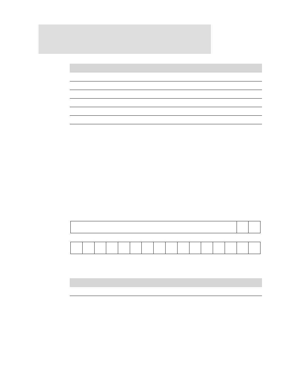
GPIO Status Registers #1 and #2 contain the status information for each of the 50
GPIO pins in the NS9750, as shown in Table 327 and Table 328. In all configurations,
the value on the GPIO input pin is brought to the Status register and the CPU has
read-only access to the register.
GPIO Status Register #2
Address: 9060 0044
Note:
The reset values for all of the status bits are undefined because they
depend on the state of the GPIO pins to NS9750.
D05
R/W
gpio5
0
gpio[5] control bit
D04
R/W
gpio4
0
gpio[4] control bit
D03
R/W
gpio3
0
gpio[3] control bit
D02
R/W
gpio2
0
gpio[2] control bit
D01
R/W
gpio1
0
gpio[1] control bit
D00
R/W
gpio0
0
gpio[0] control bit
Bits
Access
Mnemonic
Reset
Description
Table 326: GPIO Control Register #1
Bits
Access
Mnemonic
Reset
Description
D31:18
R
Not used
0x0
Always read as 0x0
D17
R
gpio49
undefined
gpio[49] status bit
Table 327: GPIO Status Register #2
13
12
11
10
9
8
7
6
5
4
3
2
1
0
15
14
31
29
28
27
26
25
24
23
22
21
20
19
18
17
16
30
gpio
49
Reserved
gpio
48
gpio
47
gpio
46
gpio
45
gpio
44
gpio
43
gpio
42
gpio
41
gpio
40
gpio
39
gpio
38
gpio
37
gpio
36
gpio
35
gpio
34
gpio
33
gpio
32