Table 420: global interrupt status register – Digi NS9750 User Manual
Page 746
U S B G l o b a l r e g i s t e r s
7 2 2
N S 9 7 5 0 H a r d w a r e R e f e r e n c e
For diagnostics, each bit serviced here can also be set to 1 by writing a 1 when the bit
is set to 0.
Note:
The DMA interrupts must be serviced in the USB DMA device block. The
FIFO interrupts must be serviced in the FIFO Interrupt Status register.
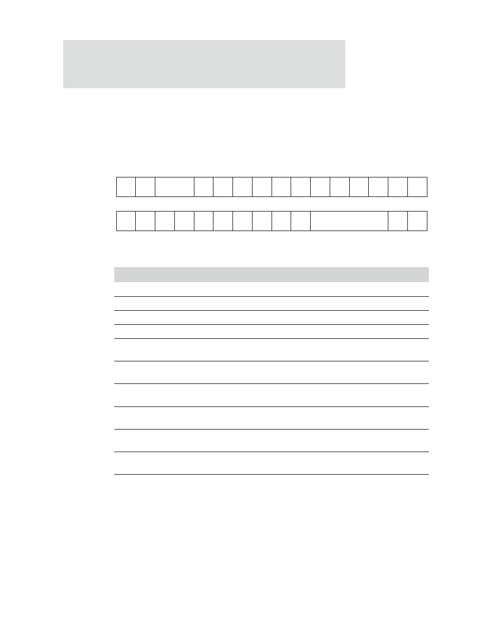
Register bit assignment
Bits
Access
Mnemonic
Reset
Description
D31
N/A
Not used
0
Always read as 0.
D30
N/A
Reserved
N/A
N/A
D29:28
N/A
Not used
0
Always read as 00.
D27
R
GBL_DMA
0
Bit-wise logical OR of the DMA# fields.
D26
R
DMA13
0
DMA channel 13 interrupt. Service in the USB DMA
block.
D25
R
DMA12
0
DMA channel 12 interrupt. Service in the USB DMA
block.
D24
R
DMA11
0
DMA channel 11 interrupt. Service in the USB DMA
block.
D23
R
DMA10
0
DMA channel 10 interrupt. Service in the USB DMA
block.
D22
R
DMA9
0
DMA channel 9 interrupt. Service in the USB DMA
block.
D21
R
DMA8
0
DMA channel 8 interrupt. Service in the USB DMA
block.
D20
R
DMA7
0
DMA channel 7 interrupt. Service in the USB DMA
block.
Table 420: Global Interrupt Status register
Rsvd
FIFO
SOF
URST
SSPND
SET
INTF
SET
CFG
WAKE
UP
Reserved
OHCI_
IRQ
Rsvd
13
12
11
10
9
8
7
6
5
4
3
2
1
0
15
14
DMA
2
DMA
1
31
29
28
27
26
25
24
23
22
21
20
19
18
17
16
30
Not used
DMA
13
GBL_
DMA
DMA
12
DMA
11
DMA
10
DMA
9
DMA
8
DMA
7
DMA
6
DMA
5
DMA
4
DMA
3
Not
used
Rsvd