1 sc140 endian support, 1 sc140 bus structure, Sc140 endian support -56 – Freescale Semiconductor StarCore SC140 User Manual
Page 88: Sc140 bus structure -56, Endian example -56

2-56
SC140 DSP Core Reference Manual
Memory Interface
•
Memory must resolve access ordering on a cycle by cycle basis. All accesses on a given cycle must
be completed before proceeding to accesses in the next cycle. Note that a conflict acces may occur
when there are multiple requests to access the same memory module, in the same cycle. An access
conflict is resolved by a stall cycle (per conflict), which serializes the multiple request.
•
Multiple access rules in a given cycle are as follows:
— Multiple read or write accesses to different memory locations execute without any
predetermined sequence.
— In cases where multiple accesses to the same memory location occur, the access sequence is
program fetch, data read, and data write.
— If two write operations access the same byte in memory in the same cycle, the operation is illegal
and the result is undefined. The same byte may be written by different but overlapping words or
long words. The memory subsystem should be able to detect these cases and issue an imprecise
interrupt to the core. The use of this interrupt is optional. Refer to
on page 5-24 for more details.
•
Accesses to non-existent memory locations are illegal and the result is undefined. The memory
subsystem can issue an imprecise interrupt to the core. The use of this interrupt is optional.
2.4.1 SC140 Endian Support
The term “little endian” is defined as a computer architecture such that given a multi-byte operand
representation, bytes at lower addresses have lower numeric significance. Each word is stored little end
first. In little endian mode, the MOVE.W D0,(R0) instruction (for example) stores bits 7–0 of D0 into
address (R0), and bits 15–8 into address (R0 + 1).
In “big endian” architectures, the most significant byte has the lowest address, and each word is stored big
end first. In big endian mode, the MOVE.W D0,(R0) instruction stores bits 15–8 of D0 into address (R0),
and bits 7–0 into address (R0 + 1).
The SC140 supports both big and little endian architectures through the big endian memory (BEM) mode
bit in the EMR. This bit samples a core input signal when exiting the reset state, and cannot be changed
during normal operation.
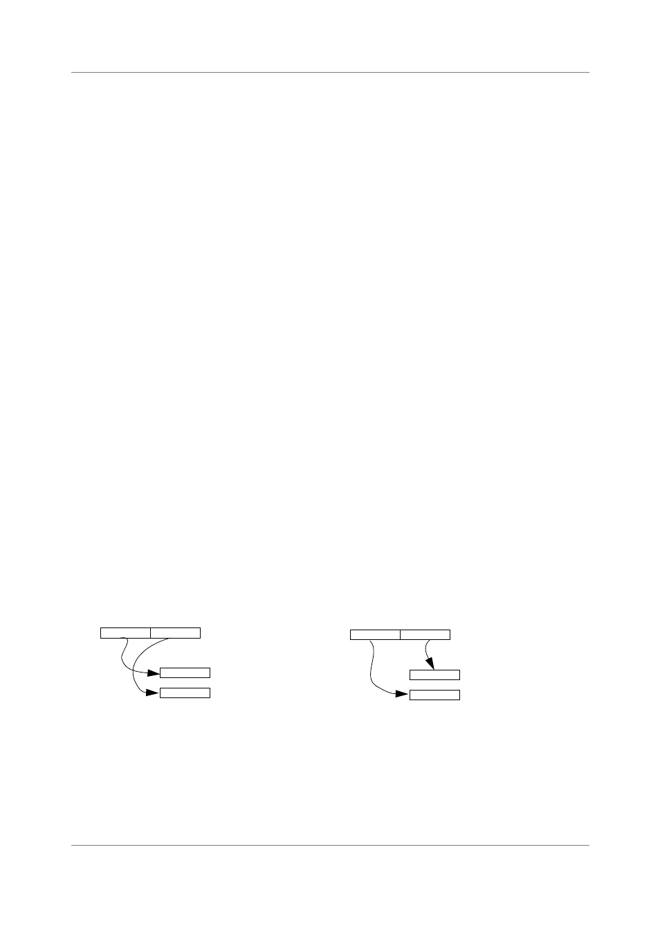
Figure 2-19 shows an example how data is transferred from a register to memory in the two endian modes.
Figure 2-19. Endian Example
2.4.1.1 SC140 Bus Structure
The entire memory space of the SC140 core is unified. The memory supports two parallel 64-bit data
accesses and one 128-bit program fetch. All can occur in parallel.
Little Endian
Big Endian
8 7
0
15
7
0
0
7
REGISTER
MEMORY
A0
A0+1
8 7
0
15
7
0
0
7
REGISTER
MEMORY
A0
A0+1
