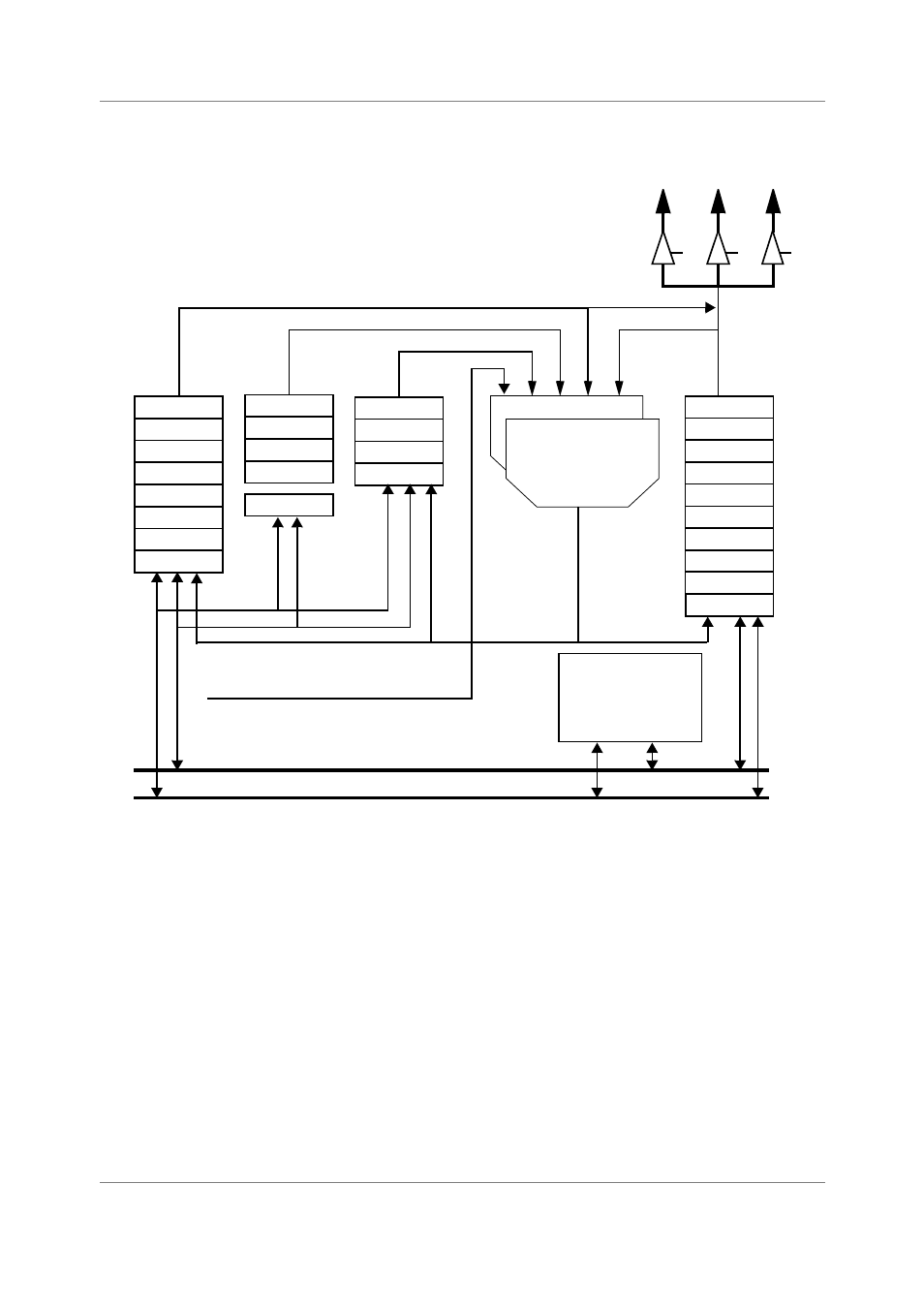
Agu block diagram -32 – Freescale Semiconductor StarCore SC140 User Manual
Page 64

2-32
SC140 DSP Core Reference Manual
Address Generation Unit
All sixteen address registers (R0–R15) as well as the NSP or ESP are used for generating addresses in the
register indirect addressing modes. All four offset registers (N0–N3) can be used by all sixteen address
registers. The four modifier registers (M0–M3) can only be used by the low bank of eight address registers
(R0–R7).
The base address (Bn) registers are uniquely associated with the low bank of Rn registers such that B0 is
used with R0, B1 with R1, and so on.
The BMU is used to perform bit mask operations such as setting, clearing, changing, or testing bits in a
destination according to an immediate mask operand. Data is loaded into the BMU over the data memory
buses XDBA or XDBB. The result is written back over XDBA or XDBB to the destinations in the next
cycle. All bit mask instructions are typically executed in two cycles and work on 16-bit data. This data can
be a memory location or a portion (high or low) of a register. For more information, see
Figure 2-12. AGU Block Diagram
Program Counter (PC) Address
R0
R1
R2
R3
R4
R5
R6
R7
N0
N1
N2
N3
PAB
XABB
XABA
NSP
MCTL
R8/B0
R9/B1
R10/B2
R11/B3
R12/B4
R13/B5
R14/B6
R15/B7
Bit
Mask
Unit
(BMU)
Memory Data Bus 1 (XDBA)
Memory Data Bus 2 (XDBB)
Address
Arithmetic
Unit (AAU)
M0
M1
M2
M3
32
32
32
64
64
ESP
