1 cascading multiple sc140 eonce modules in a soc, Cascading multiple sc140 eonce modules in a soc -2, Jtag interface signal descriptions -2 – Freescale Semiconductor StarCore SC140 User Manual
Page 112: Processing state transitions -43

4-2
SC140 DSP Core Reference Manual
Overview of the Combined JTAG and EOnCE Interface
In addition, the EOnCE:
•
Reduces system intrusion when debugging in real time.
•
Reduces the use of general-purpose peripherals for debugging I/O activities.
•
Standardizes the process of system-level debugging across multiple target platforms.
•
Provides a rich set of watchpoint features with real-time operation.
•
Provides non-intrusive access capability to peripheral registers (for read and write) while in debug
state.
•
Supports a trace buffer for program flow tracing.
•
Provides a programming model accessible during real time by either software or debugging system.
4.2 Overview of the Combined JTAG and EOnCE
Interface
The JTAG and EOnCE blocks are tightly coupled. All EOnCE registers are JTAG compliant. Three
different programming models are available when using the JTAG and EOnCE interface:
•
EOnCE programming model through a host on the JTAG port
•
EOnCE programming model through a host from the core software
•
JTAG programming model through a host on the JTAG port
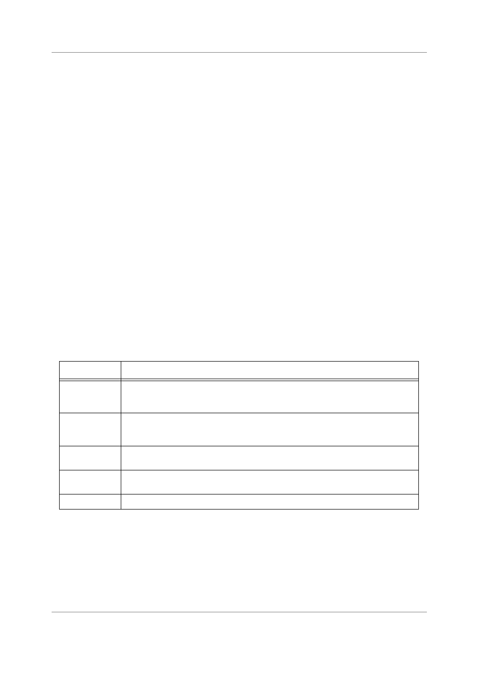
Table 4-1 lists the JTAG or EOnCE interface signals.
4.2.1 Cascading Multiple SC140 EOnCE Modules in a SoC
A typical SC140SoC uses the JTAG TAP controller for standard defined testing compatibilities and for
single/multi-core EOnCE control and EOnCE interconnection control. In a multi-core device the EOnCE
modules interconnect in a chain and are configured and controlled by the JTAG port (see Figure 4-1).
Table 4-1. JTAG Interface Signal Descriptions
Signal Name
Signal Description
TDI
Test Data Input
—
Provides a serial input data stream to the JTAG and EOnCE module. It
is sampled on the rising edge of the test clock input (TCK), and has an on-chip pull-up
resistor.
TDO
Test Data Output
—
Provides a serial tri-state capable output data stream from the JTAG
and EOnCE modules. It is driven in the Shift-IR and Shift-DR controller states of the JTAG
state machine. The signal changes on the falling edge of TCK (see below).
TCK
Test Clock Input
—
Provides a gated clock to synchronize the test logic and shift serial
data to and from the JTAG or EOnCE module.
TMS
Test Mode Select Input
—
Sequences the JTAG controller's state machine. It is sampled
on the rising edge of TCK and has an on-chip pull-up resistor.
TRST
Test Reset
—
Provides a reset signal to the JTAG TAP controller.
