Configuration, Configuration -3, Configuration page – Altera Embedded Peripherals IP User Manual
Page 60
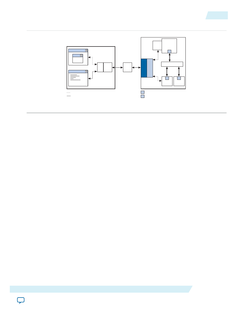
Figure 7-2: Example System Using the JTAG UART Core
PC
Interface
Host PC
JTAG
Server
Download
Cable
Altera
Downlo
Debugger
Debugger
C
Debug Data
PC
Interface
JTAG
Host PC
Altera FPGA
J
TA
G
Controller
JT
A
G
Hub
JTAG
Server
Download
Cable
Driver
Altera
Download
Cable
JTAG
Debug
Module
JTAG
UART
System Interconnect
Fabric
Character Stream
Debugger
Debugger
C
JTAG Terminal
JTAG Terminal
Nios II
Processor
On-Chip
Memory
M
S
S
M
S
Avalon-MM master port
Avalon-MM slave port
The JTAG controller on the FPGA and the download cable driver on the host PC implement a simple
data-link layer between host and target. All JTAG nodes inside the FPGA are multiplexed through the
single JTAG connection. JTAG server software on the host PC controls and decodes the JTAG data
stream, and maintains distinct connections with nodes inside the FPGA.
The example system in the figure above contains one JTAG UART core and a Nios II processor. Both
agents communicate with the host PC over a single Altera download cable. Thanks to the JTAG server
software, each host application has an independent connection to the target. Altera provides the JTAG
server drivers and host software required to communicate with the JTAG UART core.
Systems with multiple JTAG UART cores are possible, and all cores communicate via the same JTAG
interface. To maintain coherent data streams, only one processor should communicate with each JTAG
UART core.
Configuration
The following sections describe the available configuration options.
Configuration Page
The options on this page control the hardware configuration of the JTAG UART core. The default settings
are pre-configured to behave optimally with the Altera-provided device drivers and JTAG terminal
software. Most designers should not change the default values, except for the Construct using registers
instead of memory blocks option.
UG-01085
2014.24.07
Configuration
7-3
JTAG UART Core
Altera Corporation