Using the sdram manufacturer's memory model, Example configurations, Example configurations -8 – Altera Embedded Peripherals IP User Manual
Page 24: Is an aggregate of the remaining signals, such as
structured as a single, monolithic block of memory. For example, even for a system that combines two
SDRAM chips, the generic memory model is implemented as a single entity.
Using the SDRAM Manufacturer's Memory Model
If the Include a functional memory model the system testbench option is not enabled, you are
responsible for obtaining a memory model from the SDRAM manufacturer, and manually wiring the
model to the SDRAM controller pins in the system testbench.
Example Configurations
The following examples show how to connect the SDRAM controller outputs to an SDRAM chip or chips.
The bus labeled
ctl
is an aggregate of the remaining signals, such as
cas_n
,
ras_n
,
cke
and
we_n
.
The address, data, and control signals are wired directly from the controller to the chip. The result is a
128-Mbit (16-Mbyte) memory space.
Figure 2-2: Single 128-Mbit SDRAM Chip with 32-Bit Data
data 32
128 Mbits
16 Mbytes
32 data width device
SDRAM
Controller
Altera FPGA
Avalon-MM
interface
to
on-chip
logic
addr
cs_n
ctl
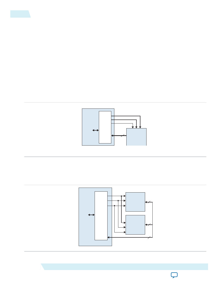
The address and control signals connect in parallel to both chips. The chips share the chipselect (
cs_n
)
signal. Each chip provides half of the 32-bit data bus. The result is a logical 128-Mbit (16-Mbyte) 32-bit
data memory.
Figure 2-3: Two 64-MBit SDRAM Chips Each with 16-Bit Data
addr
ctl
cs_n
SDRAM
Controller
Altera FPGA
Avalon-MM
interface
to
on-chip
logic
64 Mbits
8 Mbytes
16 data width device
64 Mbits
8 Mbytes
16 data width device
data
16
16
32
2-8
Using the SDRAM Manufacturer's Memory Model
UG-01085
2014.24.07
Altera Corporation
SDRAM Controller Core