Altera Embedded Peripherals IP User Manual
Page 28
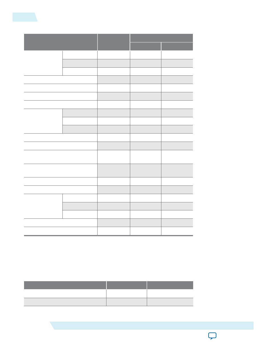
Table 2-3: Timing Parameters for Micron MT48LC4M32B2 SDRAM Device
Parameter
Symbol
Value (ns) in -7 Speed Grade
Min.
Max.
Access time
from CLK
(pos. edge)
CL = 3
t
AC(3)
—
5.5
CL = 2
t
AC(2)
—
8
CL = 1
t
AC(1)
—
17
Address hold time
t
AH
1
—
Address setup time
t
AS
2
—
CLK high-level width
t
CH
2.75
—
CLK low-level width
t
CL
2.75
—
Clock cycle
time
CL = 3
t
CK(3)
7
—
CL = 2
t
CK(2)
10
—
CL = 1
t
CK(1)
20
—
CKE hold time
t
CKH
1
—
CKE setup time
t
CKS
2
—
CS#, RAS#, CAS#, WE#, DQM
hold time
t
CMH
1
—
CS#, RAS#, CAS#, WE#, DQM
setup time
t
CMS
2
—
Data-in hold time
t
DH
1
Data-in setup time
t
DS
2
Data-out
high-
impedance
time
CL = 3
t
HZ(3)
5.5
CL = 2
t
HZ(2)
—
8
CL = 1
t
HZ(1)
—
17
Data-out low-impedance time
t
LZ
1
—
Data-out hold time
t
OH
2.5
The FPGA I/O Timing Parameters table below shows the relevant timing information, obtained from the
Timing Analyzer section of the Quartus II Compilation Report. The values in the table are the maximum
or minimum values among all device pins related to the SDRAM. The variance in timing between the
SDRAM pins on the device is small (less than 100 ps) because the registers for these signals are placed in
the I/O cell.
Table 2-4: FPGA I/O Timing Parameters
Parameter
Symbol
Value (ns)
Clock period
t
CLK
20
Minimum clock-to-output time
t
CO_MIN
2.399
2-12
Example Calculation
UG-01085
2014.24.07
Altera Corporation
SDRAM Controller Core