Functional description, Functional description -2 – Altera Embedded Peripherals IP User Manual
Page 53
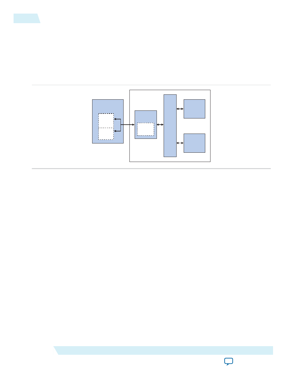
Functional Description
As shown below, the EPCS device's memory can be thought of as two separate regions:
• FPGA configuration memory—FPGA configuration data is stored in this region.
• General-purpose memory—If the FPGA configuration data does not fill up the entire EPCS device,
any left-over space can be used for general-purpose data and system startup code.
Figure 6-1: Nios II System Integrating an EPCS Serial Flash Controller Core
System Interconnect
Fab
ric
EPCS
Controller Core
Boot-Loader
ROM
EPCS Serial
Configuration
Device
Config
Memory
General-
Purpose
Memory
Nios II CPU
Other
On-Chip
Peripheral(s)
Altera FPGA
• By virtue of the HAL generic device model for flash devices, accessing the EPCS device using the HAL
API is the same as accessing any flash memory. The EPCS device has a special-purpose hardware
interface, so Nios II programs must read and write the EPCS memory using the provided HAL flash
drivers.
The EPCS serial flash controller core contains an on-chip memory for storing a boot-loader program.
When used in conjunction with Cyclone
®
and Cyclone II devices, the core requires 512 bytes of boot-
loader ROM. For Cyclone III, Cyclone IV, Stratix
®
II, and newer device families in the Stratix series, the
core requires 1 KByte of boot-loader ROM. The Nios II processor can be configured to boot from the
EPCS serial flash controller core. To do so, set the Nios II reset address to the base address of the EPCS
serial flash controller core. In this case, after reset the CPU first executes code from the boot-loader ROM,
which copies data from the EPCS general-purpose memory region into a RAM. Then, program control
transfers to the RAM. The Nios II IDE provides facilities to compile a program for storage in the EPCS
device, and create a programming file to program into the EPCS device.
For more information, refer to the Nios II Flash Programmer User Guide..
If you program the EPCS device using the Quartus
®
II Programmer, all previous content is erased. To
program the EPCS device with a combination of FPGA configuration data and Nios II program data, use
the Nios II IDE flash programmer utility.
The Altera EPCS configuration device connects to the FPGA through dedicated pins on the FPGA, not
through general-purpose I/O pins. In all Altera device families except Cyclone III and Cyclone IV, the
EPCS serial flash controller core does not create any I/O ports on the top-level Qsys system module. If the
EPCS device and the FPGA are wired together on a board for configuration using the EPCS device (in
other words, active serial configuration mode), no further connection is necessary between the EPCS
serial flash controller core and the EPCS device. When you compile the Qsys system in the Quartus II
6-2
Functional Description
UG-01085
2014.24.07
Altera Corporation
EPCS Serial Flash Controller Core