Specify delay, Data register settings, Timing settings – Altera Embedded Peripherals IP User Manual
Page 112: Data register settings -6, Timing settings -6
The actual frequency achieved will not be greater than the specified target value.
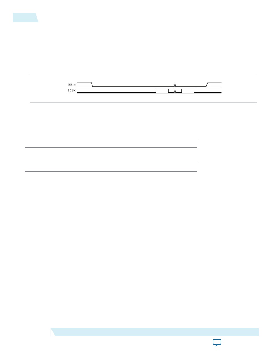
Specify Delay
Turning on this option causes the SPI master to add a time delay between asserting the
ss_n
signal and
shifting the first bit of data. This delay is required by certain SPI slave devices. If the delay option is on,
you must also specify the delay time in units of ns, µs or ms. An example is shown in below.
Figure 10-4: Time Delay Between Asserting ss_n and Toggling sclk
The delay generation logic uses a granularity of half the period of
sclk
. The actual delay achieved is the
desired target delay rounded up to the nearest multiple of half the
sclk
period, as shown in the follow two
equations.
Table 10-3:
p = 1/2 x (period of
sclk
)
Table 10-4:
Actual delay = ceiling x (desired delay/ p)
Data Register Settings
The data register settings affect the size and behavior of the data registers in the SPI core. There are two
data register settings:
• Width—This setting specifies the width of
rxdata
,
txdata
, and the receive and transmit shift
registers. The range is from 1 to 32.
• Shift direction—This setting determines the direction that data shifts (MSB first or LSB first) into and
out of the shift registers.
Timing Settings
The timing settings affect the timing relationship between the
ss_n
,
sclk
,
mosi
and
miso
signals. In this
discussion the
mosi
and
miso
signals are referred to generically as data. There are two timing settings:
• Clock polarity—This setting can be 0 or 1. When clock polarity is set to 0, the idle state for
sclk
is
low. When clock polarity is set to 1, the idle state for
sclk
is high.
• Clock phase—This setting can be 0 or 1. When clock phase is 0, data is latched on the leading edge of
sclk
, and data changes on trailing edge. When clock phase is 1, data is latched on the trailing edge of
sclk
, and data changes on the leading edge.
The following four clock polarity figures demonstrate the behavior of signals in all possible cases of
clock polarity and clock phase.
10-6
Specify Delay
UG-01085
2014.24.07
Altera Corporation
SPI Core