Altera Embedded Peripherals IP User Manual
Page 37
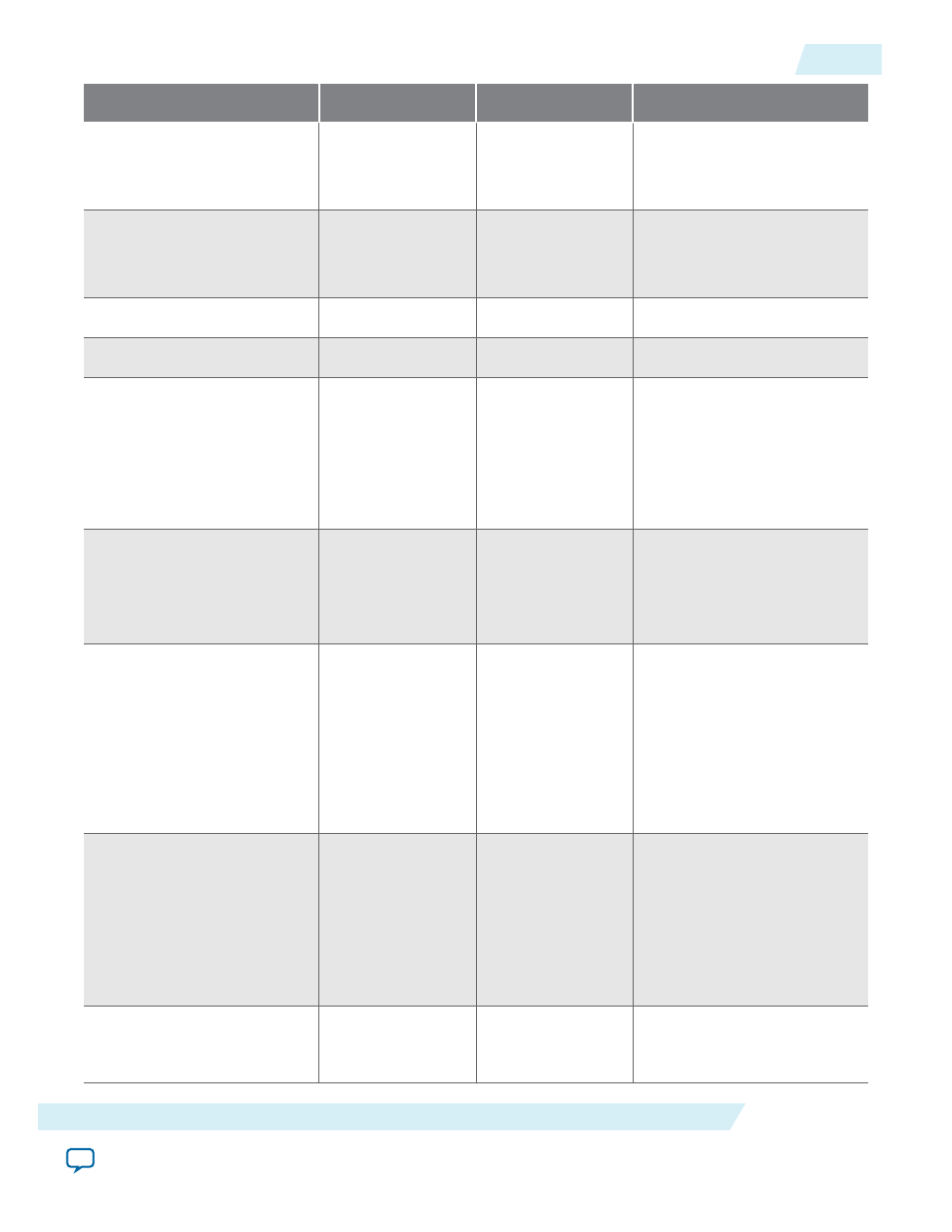
Signal
Width
Direction
Description
sdram_dq_oen
1
Output
SDRAM data bus input.
Valid only when pin-sharing
mode is enabled.
sdram_dq
sdram_data_width
Input/Output
SDRAM data bus.
Valid only when pin-sharing
mode is disabled.
sdram_addr
sdram_addr_width
Output
SDRAM address bus.
sdram_ba
sdram_bank_width
Output
SDRAM bank address.
sdram_dqm
dqm_width
Output
SDRAM data mask. When
asserted, it indicates to the
SDRAM chip that the
corresponding data signal is
suppressed. There is one
DQM line per 8 bits data
lines
sdram_ras_n
1
Output
Row Address Select. When
taken LOW, the value on the
tcm_addr_out
bus is used to
select the bank and activate
the required row.
sdram_cas_n
1
Output
Column Address Select.
When taken LOW, the value
on the
tcm_addr_out
bus is
used to select the bank and
required column. A read or
write operation will then be
conducted from that
memory location, depending
on the state of
tcm_we_out
.
sdram_we_n
1
Output
SDRAM Write Enable,
determins whether the
location addressed by
tcm_
addr_out
is written to or
read from.
0=Read
1=Write
sdram_cs_n
Output
SDRAM Chip Select. When
taken LOW, will enables the
SDRAM device.
UG-01085
2014.24.07
Interface
3-7
Tri-State SDRAM
Altera Corporation