16 pad resistive pull di, 3 gpio operation, 1 port direction control – Maxim Integrated MAXQ7667 User Manual
Page 90: 3 gpio operation -15, 1 port direction control and input/output -15, Maxq7667 user’s guide, 1 port direction control and input/output

5-15
__________________________________________________________________________________________________________
MAXQ7667 User’s Guide
5.2.16 Pad Resistive Pull Direction Register (Port 1) (PR1)
Register Description:
Pad Resistive Pull Direction Register (Port 1)
Register Name:
PR1
Register Address:
Module 00h, Index 1Ch
Bits 7 to 0: Port 1 Resistive Select Bits 7:0 (PR1[7:0]). When the port direction register PD1 configures a particular I/O pin as an
input, and the corresponding PO1 register bit enables a resistive pull, PR1 controls the direction of that pull. If the PR1 bit is set to 0,
the I/O pin has a resistive pulldown of approximately 150k
Ω (typical). When the PR1 bit is set to 1, the I/O pin has a resistive pullup of
approximately 150k
Ω (typical).
5.3 GPIO Operation
From a software perspective, the MAXQ7667 ports appear as a group of peripheral registers with unique addresses and are addressed
as a byte or 8 individual bit locations. The ports are designed to provide programming flexibility for the user application.
• All individual I/O bits are independently configured.
• Any combination of input, output, alternate, or special function in a port is permitted.
• All I/O pins have protection circuitry to DVDDIO and ground.
• When configured as input, the resistive pull direction of 150k
Ω can be controlled.
• Output strength on all I/O pins can be controlled to either 1mA (typical) or 2mA (typical).
5.3.1 Port Direction Control and Input/Output
The port direction registers (PD0 and PD1) control the MAXQ7667’s respective port pins’ (P0 and P1) input/output direction. The port
input registers (PI0 and PI1) are read-only registers that always reflect the logic state on the pins. The port output registers (PO0 and
PO1) have dual function. For pins defined as output, the port output registers store output data and for pins defined as input, the reg-
isters control whether the internal weak pullup is enabled or disabled. Table 5-3 shows the input/output states of the port pins as con-
trolled by the data direction register, output register, pad drive strength register, and pad resistive pull direction register. The table also
shows the port pins’ (P0 and P1) input/output states in standard mode (no special or alternate function enabled).
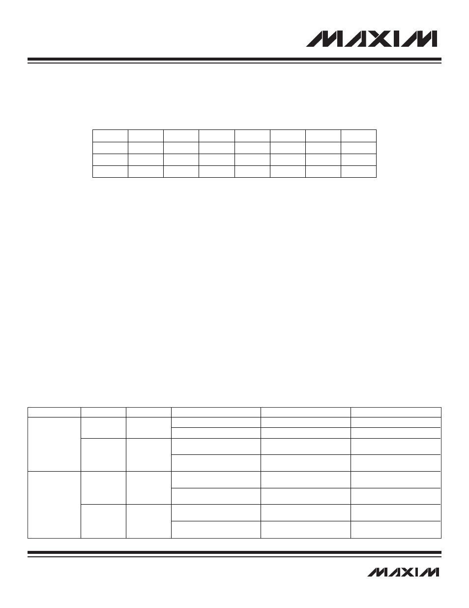
Table 5-3. Port Pin Input/Output States (in Standard Mode)
r = read, w = write
Note: This register is cleared to FFh on all forms of reset.
Bit #
7
6
5
4
3
2
1
0
Name
PR17
PR16
PR15
PR14
PR13
PR12
PR11
PR10
Reset
1
1
1
1
1
1
1
1
Access
rw
rw
rw
rw
rw
rw
rw
rw
PORT PIN MODE
PDn.x
POn.x
PRn.x
PSn.x
PORT PIN (Pn.x) STATE
X
X
Three-state
0
0
X
X
Three-state
0
(150k pulldown)
X
150k pulldown
Input
0
1
1
(150k pullup)
X
150k pullup
X
0
(1mA drive strength)
Low (1mA)
1
0
X
1
(2mA drive strength)
Low (2mA)
X
0
(1mA drive strength)
High (1mA)
Output
1
1
X
1
(2mA drive strength)
High (1mA)
n = ports, x = pins
